

Pin diode
a diode and pin technology, applied in the field of pin (p intrinsic n) diodes, can solve the problems of reducing the concentration of electric fields in the end part, unable to prevent the concentration of electric fields in the curved part of the anode region, and destroying the element thermally, so as to improve avalanche resistance, reduce productivity, and suppress current
- Summary
- Abstract
- Description
- Claims
- Application Information
AI Technical Summary
Benefits of technology
Problems solved by technology
Method used
Image

Examples
first embodiment
[0044]
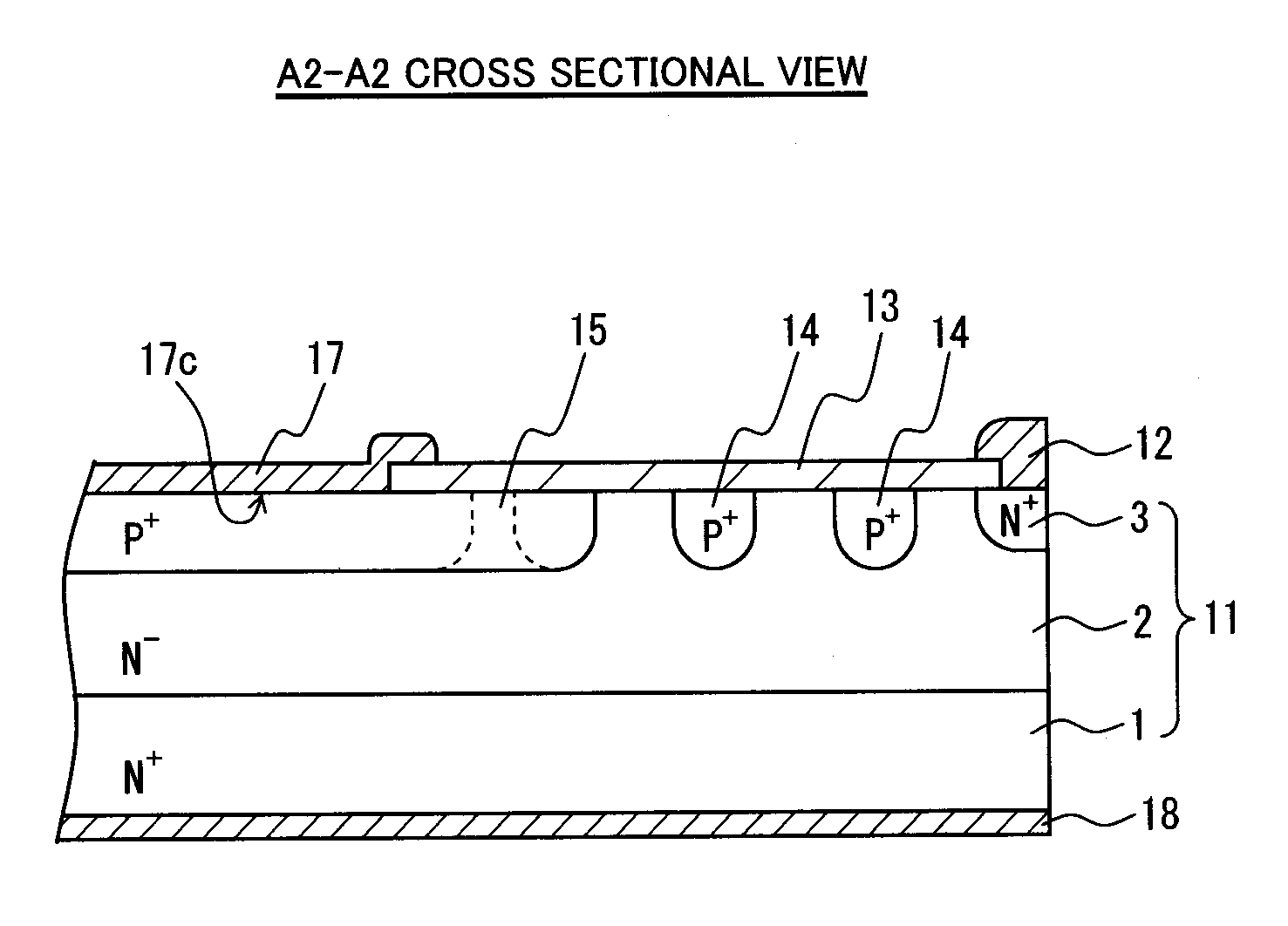
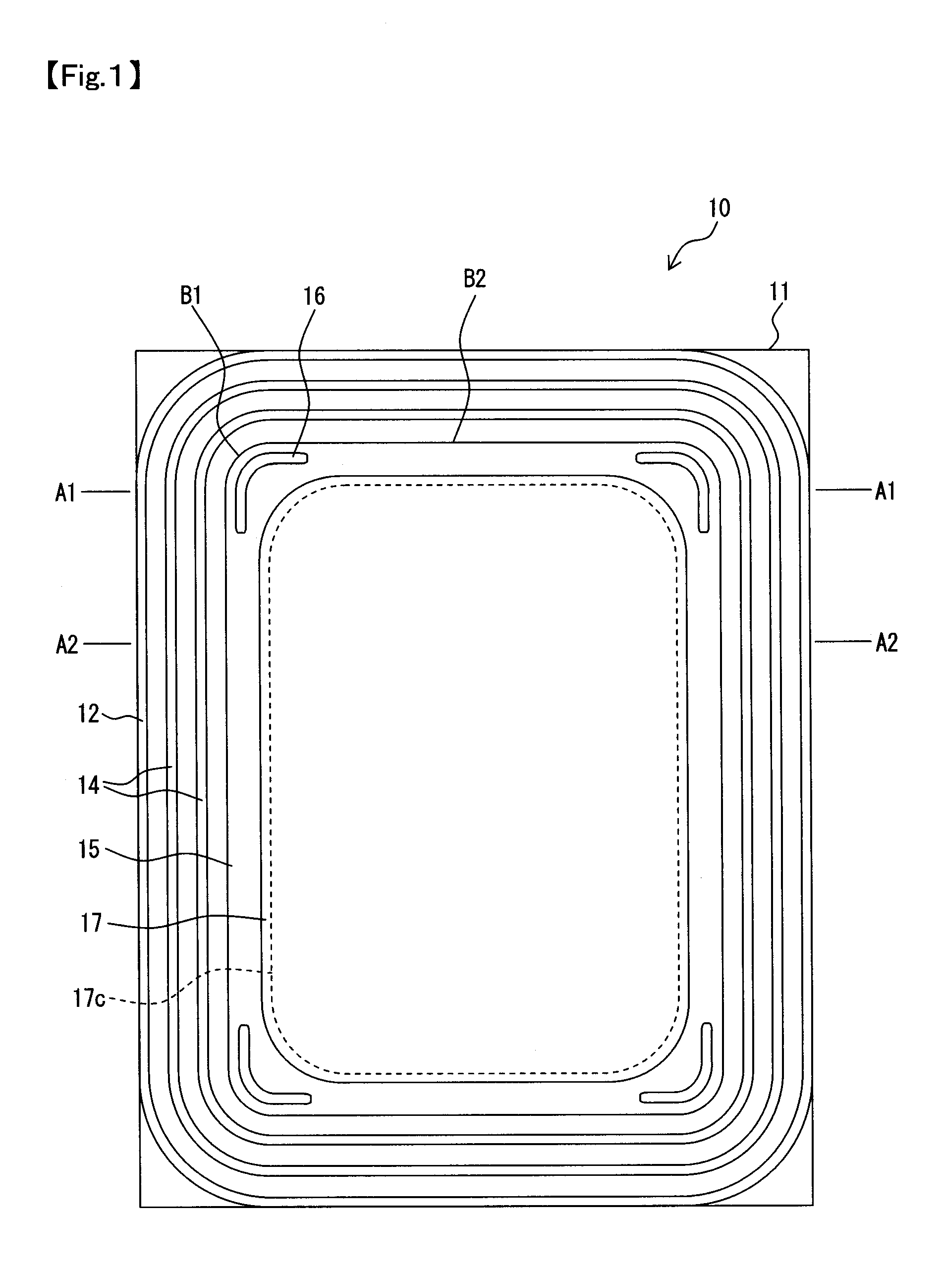
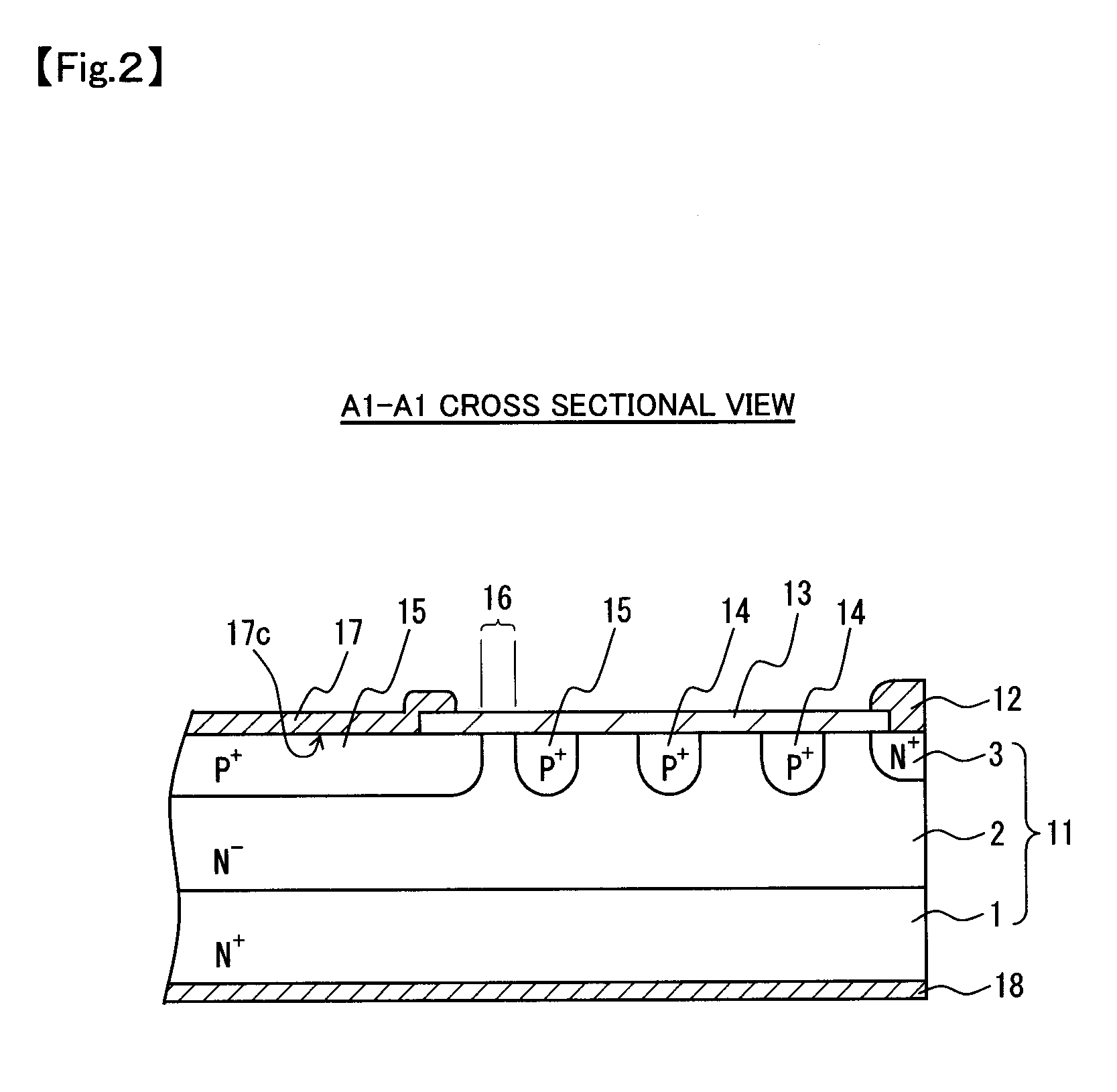
[0045]FIG. 1 is a plan view illustrating a configuration example of a PIN diode according to a first embodiment of the present invention. A PIN diode 10 is a semiconductor rectifier element including respective semiconductor layers of P-I-N, and for examples, as an FRD (Fast Recovery Diode), used for a power converter or the like.
[0046]In the PIN diode 10, by selectively diffusing P-type impurities into one principal surface of an N-type semiconductor substrate 11, two FLRs 14 and an anode region 15 are formed. Also, on the one principal surface of the semiconductor substrate 11, a substantially rectangular anode electrode 17 and an annular equipotential electrode 12 are formed through an unillustrated insulating film.
[0047]The anode region 15 is a region made of a P-type semiconductor, and has a substantially rectangular outer edge of which four sides are adapted to be linear parts B2 and four vertices are adapted to be substantially arc-like curved parts B1. Each of the FLRs...
second embodiment
[0070]In the first embodiment, described is the example of the case where, for each of the curved parts B1 of the anode region 15, the non-diffusion corner region 16 including the N− semiconductor layer 2 is formed. On the other hand, in the present embodiment, described is the case where for each of linear parts B2 of an anode region 15, a non-diffusion side region is formed on an inner side of the linear part B2.
[0071]FIG. 6 is a plan view illustrating a configuration example of a PIN diode according to the second embodiment of the present invention, in which a PIN diode 10 provided with non-diffusion corner regions 16 and the non-diffusion side regions 19 is illustrated. In the PIN diode 10, in an anode region 15 on an outer side of a contact region 17c, the non-diffusion corner regions 16 and non-diffusion side regions 19 are formed.
[0072]Each of the non-diffusion side regions 19 is a highly resistive N-type (N−) semiconductor region formed in the anode region 15; formed between...
PUM
| Property | Measurement | Unit |
|---|---|---|
| length | aaaaa | aaaaa |
| resistance | aaaaa | aaaaa |
| impurity concentration | aaaaa | aaaaa |
Abstract
Description
Claims
Application Information