

Electrostatic chuck apparatus
- Summary
- Abstract
- Description
- Claims
- Application Information
AI Technical Summary
Benefits of technology
Problems solved by technology
Method used
Image

Examples
example 1
Manufacturing of Electrostatic Chuck Apparatus
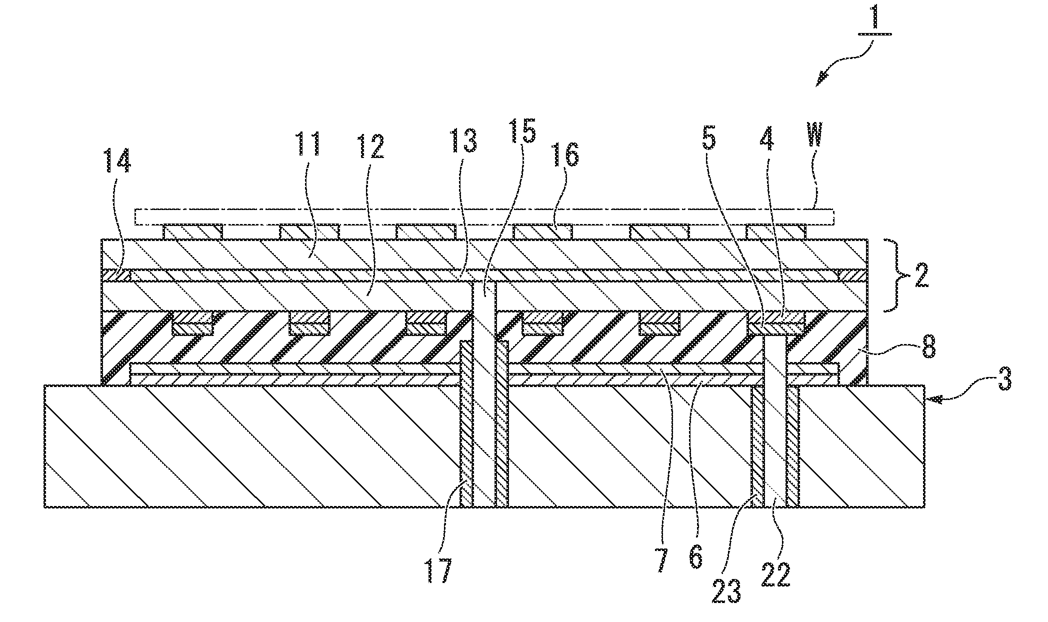
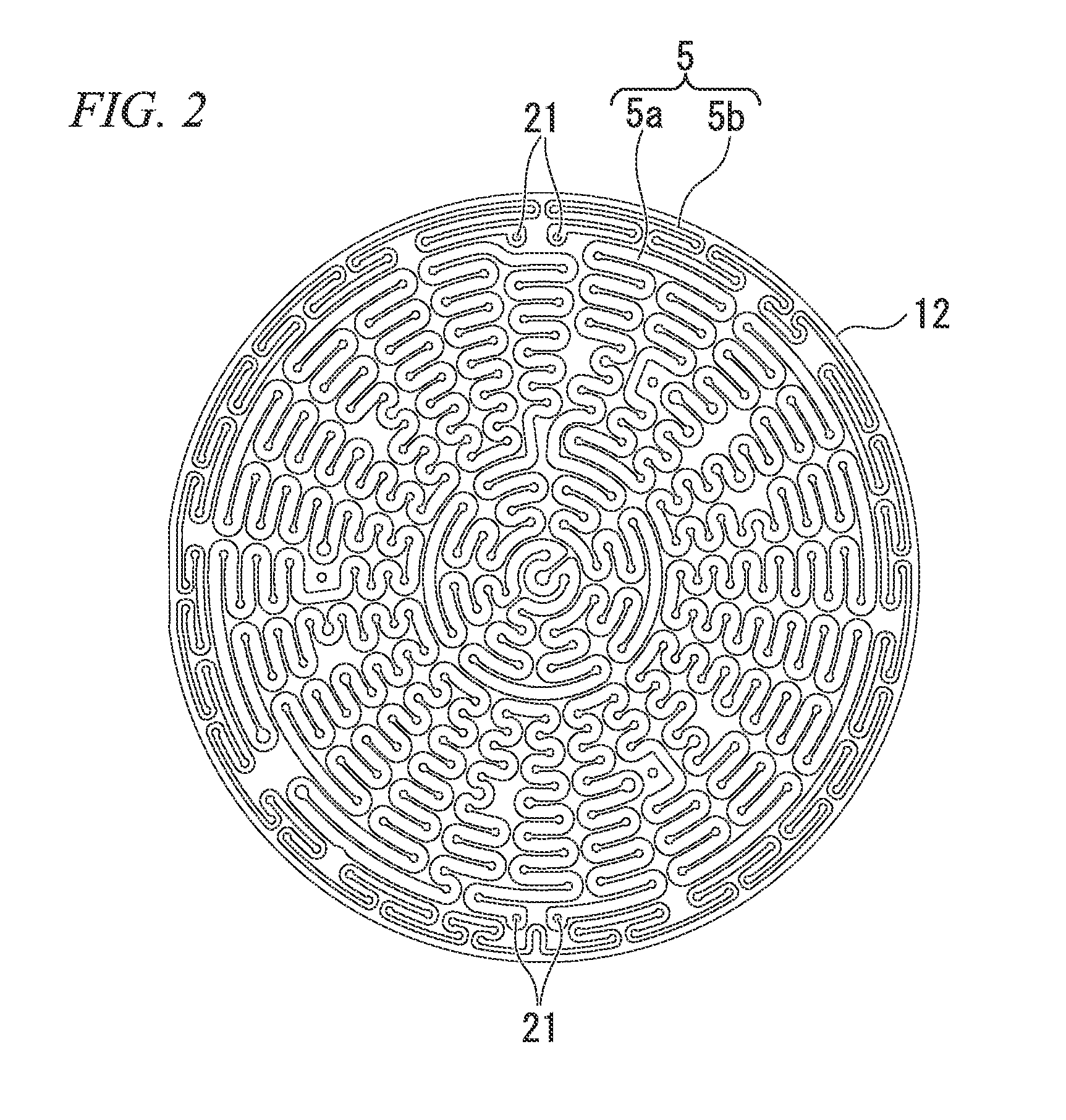
[0130]The electrostatic chuck section 2 buried with the electrostatic adsorbing internal electrode 13 having a thickness of 20 μm in an inner section thereof was manufactured by a known method.
[0131]A mounting plate 11 of the electrostatic chuck section 2 is an aluminum oxide-silicon carbide composite sintered body containing silicon carbide of 8.5% by mass, and has a disk shape with a thickness of 0.5 mm and a diameter of 298 mm. Furthermore, the electrostatic adsorption surface of the mounting plate 11 is made to concave and convex surfaces by forming a plurality of protrusion sections 16 having a height of 40 μm, the top of the protrusion section 16 is a holding surface of the plate specimen W, and a cooling gas can be caused to flow in the groove formed between the concave section and the plate specimen W electrostatically adsorbed.
[0132]Furthermore, similar to the mounting plate 11, a support plate 12 is an aluminum oxide-silicon ca...
example 2
Manufacturing of Electrostatic Chuck Apparatus
[0161]The electrostatic chuck apparatus of Example 2 was manufactured similar to Example 1, except that the mounting plate 11 and the support plate 12 of the electrostatic chuck section 2 were the yttrium oxide sintered body, and the electrostatic adsorbing internal electrode 13 was the yttrium oxide-molybdenum conductive composite sintered body.
(Evaluation)
[0162]The electrostatic chuck apparatus of Example 2 was evaluated according to Example 1.
[0163]As a consequence, in (1) the voltage endurance, the leakage current in a case of applying the voltage of 10 kV or 4 kV was equal to or less than 0.1 μA, and showed the extremely satisfactory voltage endurance. In (2) the in-plane temperature control of the silicon wafer and the temperature rising and drop characteristics, it was found that the in-plane temperature of the silicon wafer is preferably controlled within a range of ±20° C. Furthermore, in (3) in the in-plane temperature of the s...
PUM
 Abstract
Description
Claims
Application Information