Transparent conductive porous nanocomposites and methods of fabrication thereof

a technology of porous glass and composite films, applied in the direction of conductive materials, solid-state devices, non-conductive materials with dispersed conductive materials, etc., can solve the problems of low transmittance of porous glass-ito composite films, complex manufacturing methods, and high cost of manufactur

Inactive Publication Date: 2012-12-06
OBRIEN PAUL GREGORY +3
View PDF3 Cites 34 Cited by
  • Summary
  • Abstract
  • Description
  • Claims
  • Application Information

AI Technical Summary

Benefits of technology

[0017]Provided herein are conductive and transparent porous nanocomposites and methods of their fabrication. The nanocomposites are fabricated by depositing small and controlled amounts of a conductive material onto and into the pores of a nanoporous transparent matrix, thus forming a coating on internal surfaces of the nanoporous matrix and defining a conductive path within the resulting nanocomposite. The nanocomposite struc

Problems solved by technology

Secondly, a nano-architected porous film with interconnected pores is deposited onto the transparent conducting layer.
However, the transmittance of these porous glass-ITO composite films was low on account of th

Method used


Image

  • Transparent conductive porous nanocomposites and methods of fabrication thereof
  • Transparent conductive porous nanocomposites and methods of fabrication thereof
  • Transparent conductive porous nanocomposites and methods of fabrication thereof

Examples


example 1

Fabrication of Transparent Conductive Nanocomposites, Bilayers and Photonic Crystals

[0101]In order to fabricate mesoporous transparent and conducting films an approximately 100 nm thick nanoparticle film was first prepared from a solution of SiO2 nanoparticles, purchased from Aldrich (Ludox SM-30, 30 wt %) that is diluted in deionised water (3:1 deionized water / Ludox). This solution is subsequently filtered through a 0.2 μm pore Nylon syringe filter before being spin-coated onto a 0.7 mm thick ·2.5 cm×2.5 cm Corning 1737 glass substrate at speed of 3000 rpm for 20 seconds. The SiO2 nanoparticle films are then annealed at 450° C. for 15 minutes in order to evaporate any remaining solvent. Subsequently, small and controlled amounts of ITO are deposited onto the SiO2 nanoparticle films in a custom built sputtering system (Kurt J. Lesker Co.) by RF magnetron sputtering from a ceramic In2O3:SnO2 target (90:10 wt %).

[0102]During the deposition, argon was flowed into the chamber at a rate ...

example 2

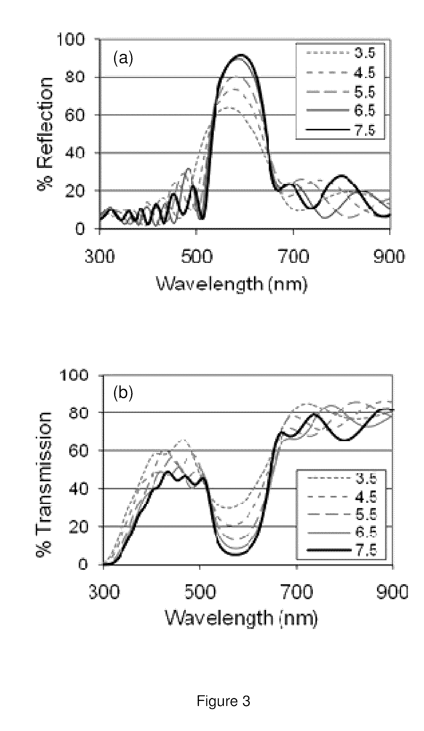
Morphology, Optical Transmission and Reflection Spectra of Multilayer Nanocomposite Films and Photonic Crystals

[0107]Experiments were performed for which either about 5 nm, or 10 nm of ITO was sputtered onto the SiO2 nanoparticle films (that is, if the ITO had been sputtered onto a flat substrate the thickness of the film would be approximately 5 nm or 10 nm thick, respectively). This process, wherein a SiO2 nanoparticle film is deposited and subsequently controlled amounts of ITO are sputtered onto the film can be successively repeated in order to build up a film of desired thickness.

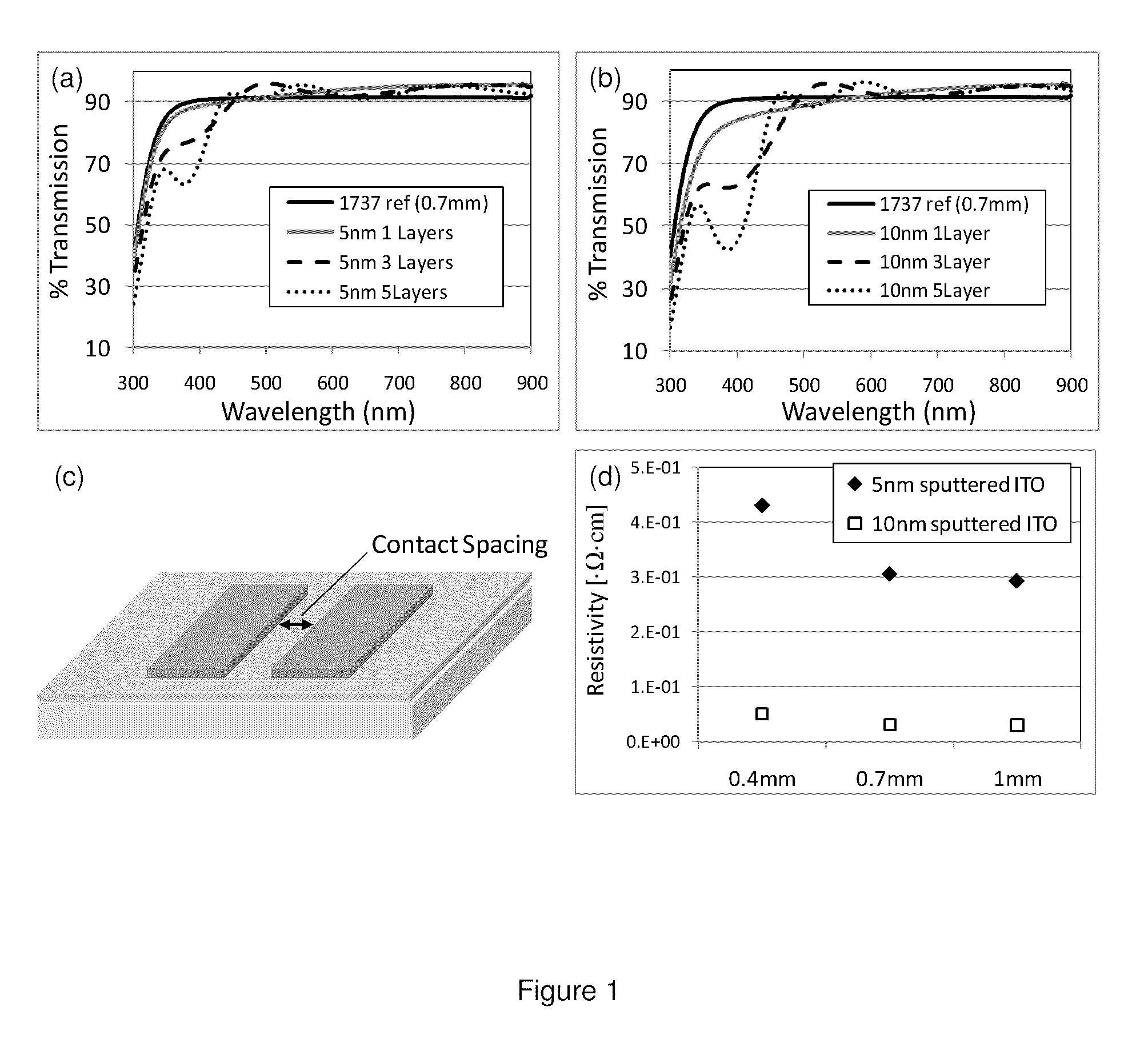
[0108]The transmission and sheet resistance of SiO2 nanoparticle films fabricated by performing the aforementioned procedure one, three and five times are shown in FIG. 1. It is interesting to note that the transmission through the Corning 1737 glass substrates that had the nanoparticle films deposited onto them is actually greater than the bare glass substrates. This is because the index of refraction...

example 3

Conductivity of Multilayer Nanocomposite Films

[0113]Conductivity measurements were obtained by depositing two rectangular co-planar aluminum contacts (0.25 cm×0.5 cm), spaced apart by 400 μm, 700 μm, or 1 mm, onto each sample. The current through the films was measured, using a Keithley 6517 electrometer, as different biases were applied across the pair of contacts. The resistivity values are calculated from the sheet resistance measurements using the formula Rs=ρ / t. Where t is the thickness of the photonic crystal and is estimated from the cross-sectional SEM images.

[0114]Referring again to FIG. 1, the resistivity of the silica nanoparticle films that underwent about 5 nm and 10 nm of ITO sputtering is approximately 3×10⁻¹ and 3×10⁻² Ω·cm, respectively. In comparison, the resistivity of an ITO film deposited using the same conditions is about 5×10⁻⁴ Ω·cm. Also, it can be noted that the resistivity of a SiO2 nanoparticle film that has not been subjected to ITO sputtering was measure...


PUM

PropertyMeasurementUnit
Pore sizeaaaaaaaaaa
Auxiliary magnetic fieldaaaaaaaaaa
Thicknessaaaaaaaaaa

Abstract

A nanocomposite material that is both transparent and electrically conductive is provided. The nanocomposite comprises a nanoporous matrix, preferably formed from nanoparticles, that is internally coated with a transparent conductive material to define an internal conductive path within the nanocomposite. The nanocomposite is substantially transparent over a defined spectral range that preferably includes at least a portion of the visible spectrum, and preferably comprises pores with a mean diameter of less than approximately 25 nm. A bilayer may be formed by depositing a layer of a transparent conductive material on top of a nanocomposite layer, or by depositing a second layer of a nanocomposite having different optical properties. The nanocomposites formed using a combination of sequential and/or concurrent deposition techniques are correspondingly discrete and/or continuously varying structures. Multilayer structures, such as photonic crystal reflectors, may be formed by depositing multiple bilayers, and integrated into devices such as tandem solar cells.

Description

CROSS-REFERENCE TO RELATED APPLICATION[0001]This application claims priority to U.S. Provisional Application No. 61 / 252,457, titled “SELECTIVELY TRANSPARENT AND CONDUCTING PHOTONIC CRYSTALS” and filed on Oct. 16, 2009, the entire contents of which are incorporated herein by reference.FIELD OF THE INVENTION[0002]The invention relates to transparent conductive porous nanocomposites and optical devices employing conductive transparent layers.BACKGROUND OF THE INVENTION[0003]Nanoporous, transparent and conducting films are a novel class of materials that exhibit a unique combination of material properties including transparency, conductivity, well-defined three-dimensional porosity and a large specific surface area. Their built-in continuous network of nanoscale voids provides two distinct advantages over conventional solid thin-film transparent conducting oxides (TCOs). Firstly, their continuously interconnected pore volume can be infiltrated with numerous different reactive species to...

Claims


Application Information

Patent Timeline
IPC IPC(8): B32B3/26H01B1/04H01B1/08B05D5/12H01L33/60H01L31/06H01L31/0232H01B1/00H01B1/22B82Y30/00
CPCC03C17/006H02S40/44C25B1/003H01B1/08H01L31/022466H01L31/03685H01L31/03762H01L31/072H01L31/0725H01L33/46H01L51/5206H01L51/5265H05B33/28Y02E10/548Y02E10/60Y02E60/366Y02E10/52Y02E10/545H01L31/056C03C2217/425H01L31/022475Y10T428/249953Y02E60/36C25B1/55H10K50/81H10K50/816H10K50/852H10K2102/331
Inventor O'BRIEN, PAUL GREGORYPUZZO, DANIEL P.KHERANI, NAZIR PYARALIOZIN, GEOFFREY ALANCHUTINAN, ALONGKARNLU, ZHENG-HONGHELANDER, MICHAEL G.
Owner OBRIEN PAUL GREGORY
Why Eureka
Try Eureka