Light emitting element, light source device, and projection display device

a technology of light source device and light emitting element, which is applied in the direction of instruments, semiconductor devices, projectors, etc., can solve the problems of low literature 1 has drawbacks, and the emission angle of light that is emitted from the light emitting element cannot be narrowed to less than 15°, so as to improve the directivity of emission light, the effect of high luminance and improved directivity

Inactive Publication Date: 2012-12-13
NEC CORP
View PDF2 Cites 23 Cited by
  • Summary
  • Abstract
  • Description
  • Claims
  • Application Information

AI Technical Summary

Benefits of technology

[0015]An object of the present invention is to provide a light emitting element that can solve the forgoing engineering problems and also provides a light source device and a projection display device that are equipped with such a light emitting element.
[0019]According to the present invention, since both luminance and directivity of emission light can be improved, a light emitting element that has high luminance and high directivity can be realized.

Problems solved by technology

Although this structure can achieve high luminance, it cannot narrow the emission angle of light that is emitted from the light emitting element to less than ±15°.
In other words, the light emitting element described in Patent Literature 1 has a drawback in which the directivity of emission light is low.
Thus, there is a problem in which, even if the light emitting element described in Patent Literature 2 is applied to an LED projector, sufficient luminance can not be obtained.

Method used


Image

  • Light emitting element, light source device, and projection display device
  • Light emitting element, light source device, and projection display device
  • Light emitting element, light source device, and projection display device

Examples


first embodiment

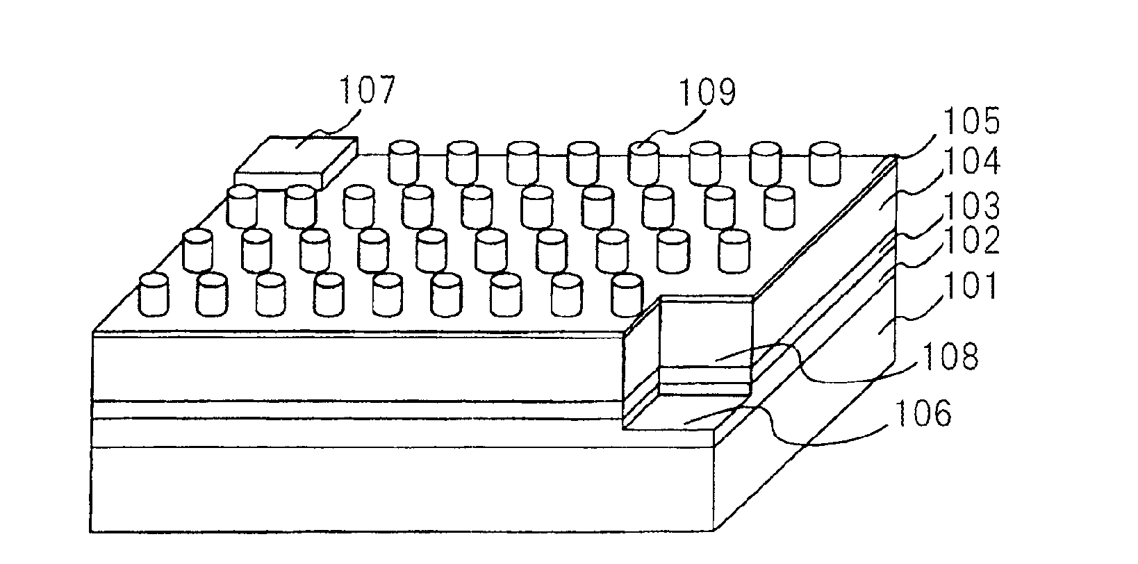
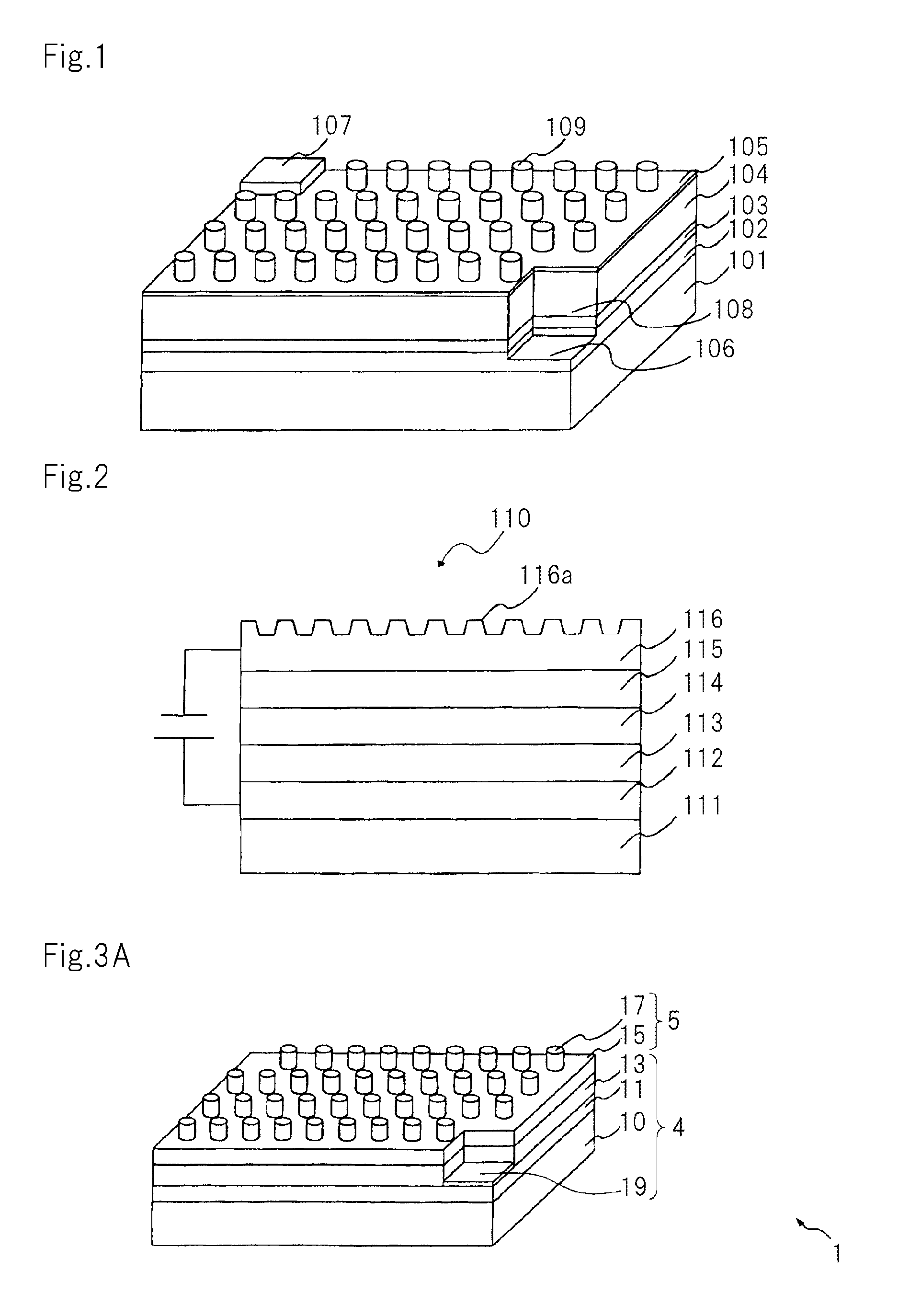
[0054]FIG. 3A is a perspective view schematically showing the structure of a light emitting element according to a first embodiment of the present invention. FIG. 3B is a plan view schematically showing the light emitting element according to this embodiment. Since the individual layers of the light emitting element are very thin and their thickness largely differ, it is difficult to illustrate the individual layers in the exact scales. Thus, the drawings do not illustrate the individual layers in the exact scales, but schematically illustrate them.

[0055]As shown in FIG. 3A, light emitting element 1 according to the first embodiment has light source layer 4 and directivity controlling layer 5 that is stacked on light source layer 4 and that operates as an optical element layer into which light emitted from light source layer 4 enters.

[0056]Light source layer 4 has substrate 10 and a pair of hole transport layer 11 and electron transport layer 13 that are formed on substrate 10. Stac...

second embodiment

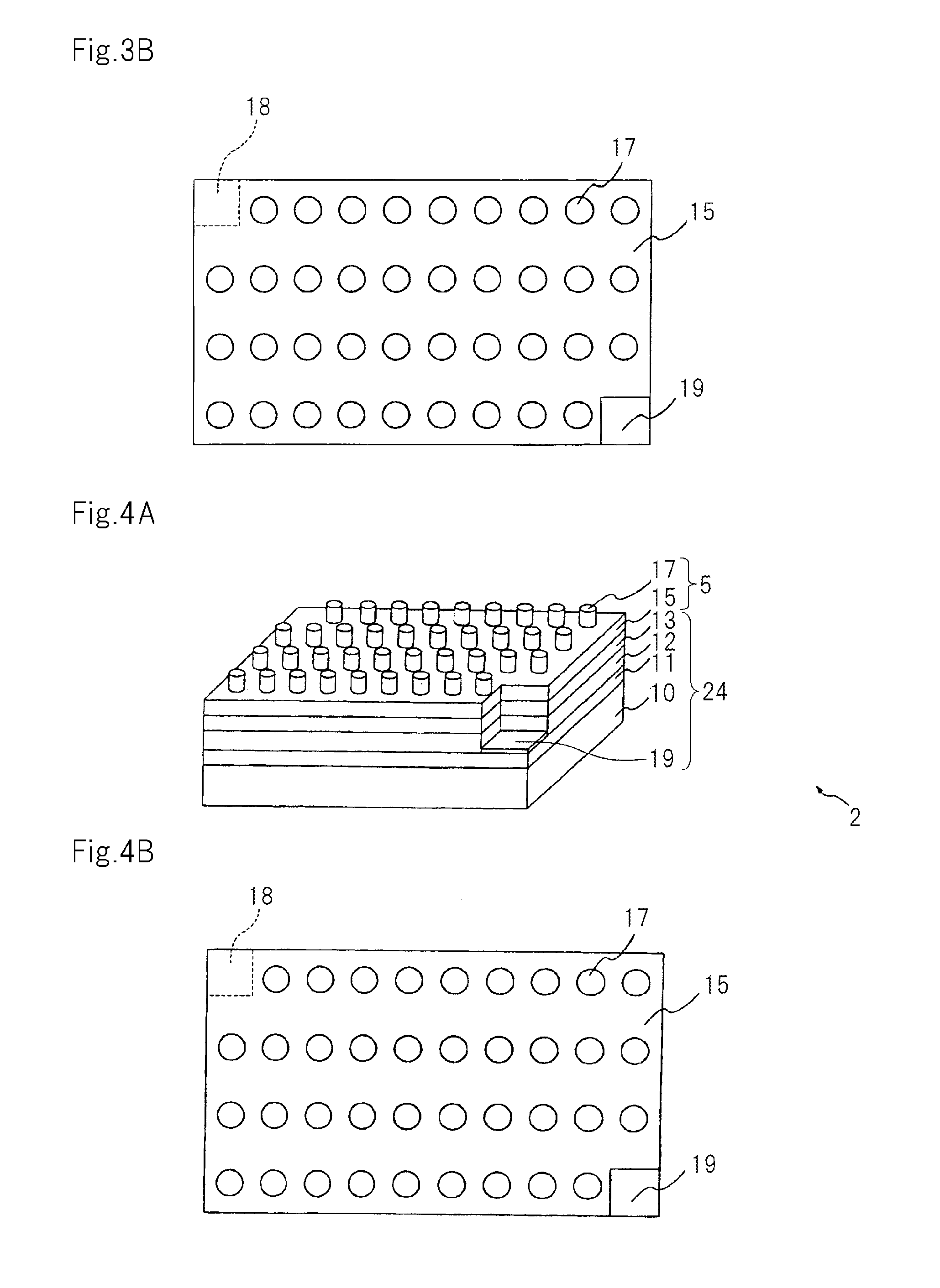
[0085]FIG. 4A is a perspective view schematically showing a light emitting element according to a second embodiment of the present invention. FIG. 4B is a plan view schematically showing the light emitting element according to the second embodiment.

[0086]As shown in FIG. 4A and FIG. 4B, light emitting element 2 according to the second embodiment has light source layer 24 and directivity controlling layer 5 that is stacked on light source layer 24 and into which light emitted from light source layer 24 enters. Since directivity controlling layer 5 of light emitting element 2 according to the second embodiment is the same as that according to the first embodiment, the description of directivity controlling layer 5 will be omitted. Light source layer 24 of light emitting element 2 according to the second embodiment is different from light source layer 4 according to the first embodiment only in that active layer 12 is formed between hole transport layer 11 and electron transport layer ...

third embodiment

[0094]FIG. 6A is a perspective view schematically showing a light emitting element according to a third embodiment of the present invention. FIG. 6B is a plan view schematically showing the light emitting element according to the third embodiment.

[0095]As shown in FIG. 6A and FIG. 6B, light emitting element 3 according to the third embodiment has light source layer 34 and directivity controlling layer 5 that is stacked on light source layer 34 and into which light emitted from light source layer 34 enters. Since directivity controlling layer 5 of light emitting element 3 according to the third embodiment is the same as that according to the firth embodiment, the description of directivity controlling layer 5 will be omitted. Light source layer 34 of light emitting element 3 according to the third embodiment is different from light source layer 24 according to the second embodiment in that anode layer 29, that is an anode, is formed completely between substrate 10 and hole transport ...


PUM


Abstract

The present invention includes light source layer (4) and directivity controlling layer (5) into which light emitted from light source layer (4) enters. Light source layer (4) has a pair of hole transport layer (11) and electron transport layer (13) formed on substrate (10). Directivity controlling layer (5) has plasmon excitation layer (15) that is laminated on non-substrate (10) side of light source layer (4) and that has a higher plasma frequency than light emitted from light source layer (4) and wave number vector conversion layer (17) that converts surface plasmons that are generated in plasmon excitation layer (15) into light having a predetermined emission angle and emits the light having the predetermined emission angle. Plasmon excitation layer (15) is sandwiched between two layers having dielectricity. The effective dielectric constant of the incident side portion including the entire structure laminated on light source layer (4) side of plasmon excitation layer (15) is greater than that of the emission side portion including the entire structure laminated on wave number vector conversion layer (17) side of plasmon excitation layer (15) and a medium that contacts wave number vector conversion layer (17).

Description

TECHNICAL FIELD[0001]The present invention relates to a light emitting element, a light source device, and a projection display device that use surface plasmons to emit light.BACKGROUND ART[0002]An LED projector that uses a light emitting diode (LED) as a light emitting element for a light source has been proposed. The LED projector of this type has an illumination optical system into which light emitted from the LED enters; a light valve having a liquid crystal display panel into which light emitted from the illumination optical system enters and a DMD (Digital Micromirror Device); and a projection optical system that projects light emitted from the light valve to a projection plane.[0003]A requirement for the LED projector is that be a minimum of optical loss in the optical path from the LED to the light valve so as to improve the luminance of projected images.[0004]In addition, as described in Non-Patent Literature 1, the LED projector is restricted by the etendue that depends on...

Claims


Application Information

Patent Timeline
Patent Type & Authority Applications(United States)
IPC IPC(8): H01L33/58G03B21/14
CPCH01L33/04H01L2933/0016H01L51/5268H01L33/58H10K50/854
Inventor NATSUMEDA, MASANAOIMAI, MASAOSUZUKI, NAOFUMITOMINAGA, SHIN
Owner NEC CORP
Why Eureka
Try Eureka