Methods and apparatus for controlling photoresist line width roughness with enhanced electron spin control

Inactive Publication Date: 2012-12-20
APPLIED MATERIALS INC
View PDF6 Cites 250 Cited by
  • Summary
  • Abstract
  • Description
  • Claims
  • Application Information

AI Technical Summary

Benefits of technology

[0010]In another embodiment, a method for controlling line width roughness of a photoresist includes providing a substrate having a patterned photoresist layer in a processing chamber, supplying a gas mixture into the processing chamber, generating a plasma in the gas mixture having electrons moving in a circular mode from the gas mixture, generating a magnetic field to enhance the electrons in the plasma moving in the circular mode to a substrate surface, and trimming an edge profile of the patterned photoresist layer disposed on the substrate surface with the enhanced electrons.
[0011]In another embodiment, a method for controlling line width roughness of a photoresist layer disposed on a substrate includes providing a substrate having a patterned photoresist layer disposed thereon into a processing chamber, supplying a gas mixture into the processing chamber, generating a plasma in the gas mixture, extracting electrons out of the plasma, generating a magnetic field to enhance the electrons moving in a circular mode to a substrate surface, and trimming an edge profile

Problems solved by technology

Integrated circuits have evolved into complex devices that can include millions of components (e.g., transistors, capacitors and resistors) on a single chip.
Accordingly, lithography processes have become more and more challenging to transfer even smaller features onto a substrate precisely and accurately without damage.
However, at such small dimensions, the roughness of the edges of a photoresist layer ha

Method used


Image

  • Methods and apparatus for controlling photoresist line width roughness with enhanced electron spin control
  • Methods and apparatus for controlling photoresist line width roughness with enhanced electron spin control
  • Methods and apparatus for controlling photoresist line width roughness with enhanced electron spin control

Examples


Embodiment Construction

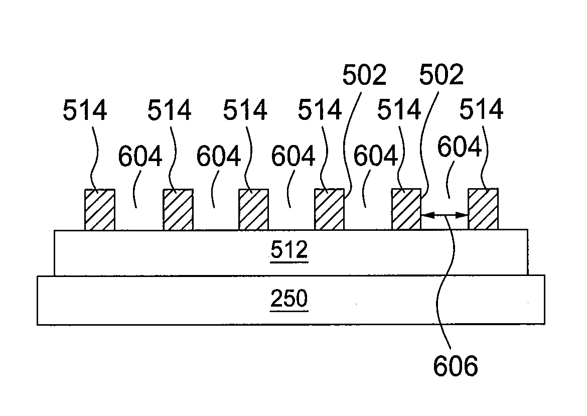
[0026]Embodiments of the present invention include methods and apparatus for controlling LWR of a photoresist layer disposed on a substrate. The LWR of a photoresist layer may be controlled by performing an ICP process with enhanced electron spin control on a photoresist layer after an exposure / development process. The ICP process is performed to provide a chemical and electron grinding process on a nanometer scale with enhanced electron spin control to smooth the edge of the photoresist layer pattern with sufficient electron spin momentum, thereby providing a smooth pattern edge of the photoresist layer with minimum pattern edge roughness for subsequent etching processes. The ICP process with enhanced electron spin control may also be used to etch a target material disposed underneath the photoresist layer on the substrate subsequent to the photoresist line edge roughness minimization process.

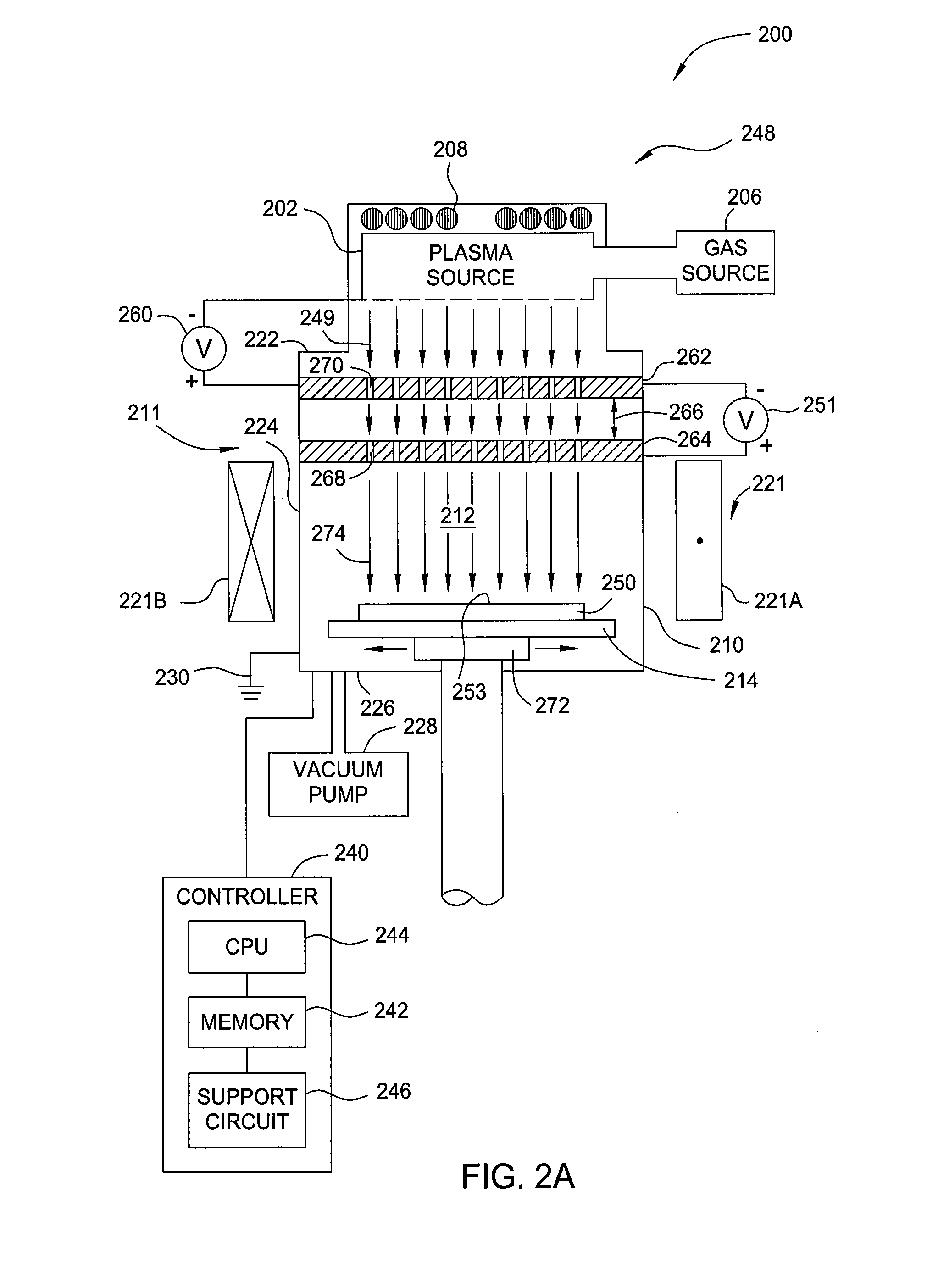
[0027]FIG. 2A depicts a schematic, cross-sectional diagram of one embodiment of an ICP rea...


PUM

PropertyMeasurementUnit
Poweraaaaaaaaaa
Magnetic fieldaaaaaaaaaa
Circumferenceaaaaaaaaaa

Abstract

The present invention provides methods and an apparatus for controlling and modifying line width roughness (LWR) of a photoresist layer with enhanced electron spinning control. In one embodiment, an apparatus for controlling a line width roughness of a photoresist layer disposed on a substrate includes a processing chamber having a chamber body having a top wall, side wall and a bottom wall defining an interior processing region, a support pedestal disposed in the interior processing region of the processing chamber, and a plasma generator source disposed in the processing chamber operable to provide predominantly an electron beam source to the interior processing region.

Description

CROSS REFERENCE TO RELATED APPLICATION[0001]This application claims benefit of U.S. Provisional Patent Application No. 61 / 497,370, filed Jun. 15, 2011, which is incorporated by reference in its entirety.BACKGROUND[0002]1. Field of the Invention[0003]The present invention generally relates to methods and apparatus for controlling photoresist line width roughness and, more specifically, to methods and apparatus for controlling photoresist line width roughness with enhanced electron spin control in semiconductor processing technologies.[0004]2. Description of the Related Art[0005]Integrated circuits have evolved into complex devices that can include millions of components (e.g., transistors, capacitors and resistors) on a single chip. The evolution of chip designs continually requires faster circuitry and greater circuit density. The demands for greater circuit density necessitate a reduction in the dimensions of the integrated circuit components.[0006]As the dimensions of the integrat...

Claims


Application Information

Patent Timeline
IPC IPC(8): B44C1/22B05C13/00
CPCH01L21/0273H01J37/32669H01J37/32422H01L21/31144H01J37/32009H01J37/3244
Inventor WU, BANQIUKUMAR, AJAYRAMASWAMY, KARTIKNALAMASU, OMKARAM
Owner APPLIED MATERIALS INC
Why Eureka
Try Eureka