Field emission panel, liquid crystal display and field emission display having the same

a field emission display and liquid crystal display technology, applied in the manufacture of electric discharge tubes/lamps, discharge tubes luminescnet screens, instruments, etc., can solve the problems of shortened lifespan of field emission panels, disadvantageous fabrication time and cost, etc., and achieve the effect of reducing fabrication time and cost and increasing lifespan

Inactive Publication Date: 2012-12-20
SAMSUNG ELECTRONICS CO LTD
View PDF11 Cites 4 Cited by
  • Summary
  • Abstract
  • Description
  • Claims
  • Application Information

AI Technical Summary

Benefits of technology

[0009]Exemplary embodiments according to the present inventive concept have been made to address at least the above problems and/or disadvantages and to provide at least the advantages described below. Accordingly, an

Problems solved by technology

However, since conventional methods for forming the above-described accommodation grooves typically include processes for forming the insulating layer and for performing the exposure and etching, such methods are disadvantageous in fabrication time and cost.
Further, becaus

Method used


Image

  • Field emission panel, liquid crystal display and field emission display having the same
  • Field emission panel, liquid crystal display and field emission display having the same
  • Field emission panel, liquid crystal display and field emission display having the same

Examples


Embodiment Construction

[0041]Hereinafter, exemplary embodiments according to the present inventive concept are described in detail with reference to the accompanying drawings.

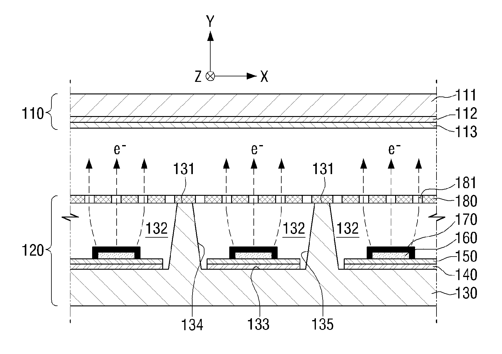
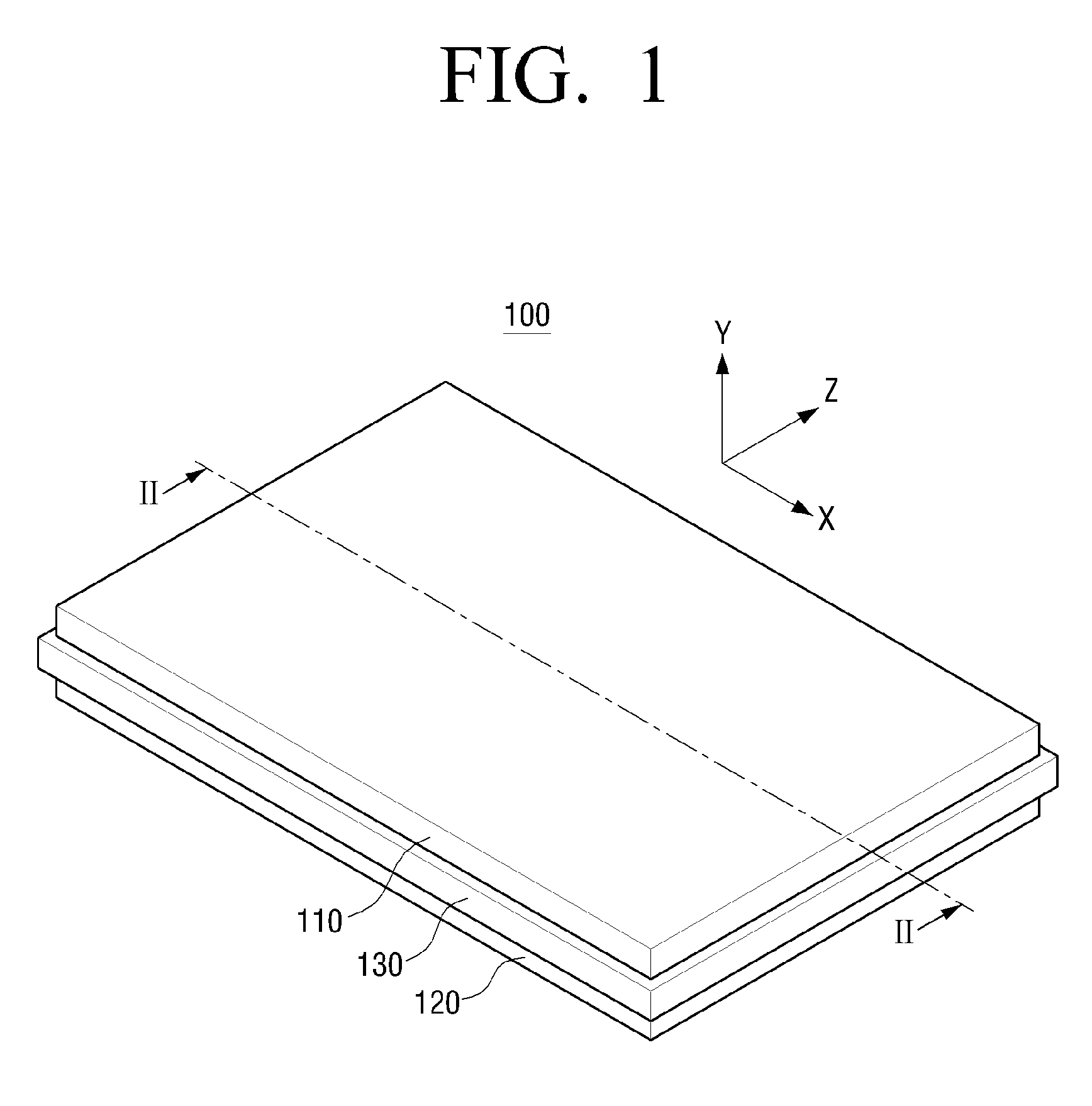
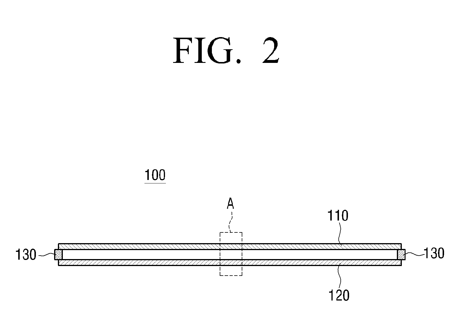
[0042]First, FIGS. 1 to 4 are referenced. FIG. 1 is a schematic perspective view illustrating a field emission panel according to an exemplary embodiment, and FIG. 2 is a schematic cross-sectional view cut along line II-II as shown in FIG. 1. FIG. 3A is an enlarged cross-sectional view illustrating an example of an area A as shown in FIG. 2, and FIG. 3B is an enlarged cross-sectional view illustrating another example of an area A as shown in FIG. 2.

[0043]A field emission panel 100 includes an upper plate 110, a lower plate 120, and a sealing member 130. The upper plate 110 and the lower plate 120 are arranged in parallel to each other, and are spaced apart from each other. The sealing member 130 is adhered to the upper plate 110 and the lower plate 120 by seal frits to seal a space between the upper plate 110 and the lower plate 120....


PUM


Abstract

A field emission panel, a liquid crystal display and a field emission display having the same are provided. The field emission panel includes a lower plate emitting electrons and an upper plate generating white light or a color image through collision with the electrons. The lower plate includes plural field emission elements, plural cathode electrodes and plural gate electrodes forming an electric field for electron emission from the electron emission elements, and a glass plate supporting the electron emission elements, the cathode electrodes, and the gate electrodes. The gate electrodes are arranged on an upper surface of the glass plate, and the glass plate has plural accommodation grooves for accommodating the plural electron emission elements and the plural cathode electrodes.

Description

PRIORITY[0001]This application claims priority under 35 U.S.C. §119(a) from Korean Patent Application No. 10-2011-0059166, filed on Jun. 17, 2011 in the Korean Intellectual Property Office, the disclosure of which is incorporated herein by reference in its entirety.BACKGROUND[0002]1. Technical Field[0003]Apparatuses and methods consistent with exemplary embodiments of the present inventive concept relate to a field emission panel, a liquid crystal display and a field emission display having the same.[0004]2. Description of the Related Art[0005]A field emission material is a material that emits electrons if an electric field is formed around the material in a vacuum atmosphere. A representative example of a field emission material is a carbon nano tube (CNT). A panel that generates light using such a field emission material can be fabricated and applied to a backlight unit of a liquid crystal display (LCD) and an image implementation panel of a field emission display (FED). Hereinaft...

Claims


Application Information

Patent Timeline
IPC IPC(8): H01J19/42H01J9/18
CPCG02F1/133602G02F2001/133625H01J63/06H01J2329/863H01J29/864H01J31/127H01J2329/861H01J29/86G02F1/133625G02F1/1335H01J1/30
Inventor SHIN, JONG-HOONKIM, HUN-SOOLEE, SANG-JINRHEE, JONG-HANPARK, JUNG-HYUN
Owner SAMSUNG ELECTRONICS CO LTD
Why Eureka
Try Eureka