Apparatus and method for measuring charge density distribution

a charge density and apparatus technology, applied in the field of apparatus and a method for measuring charge density distribution, can solve the problems of severe limitations in the scan area and scan speed, insufficient to image a whole fingerprint, and insufficient to achieve the effect of 5 hours of scan tim

Active Publication Date: 2012-12-20
THE UNIV OF SUSSEX
View PDF15 Cites 22 Cited by
  • Summary
  • Abstract
  • Description
  • Claims
  • Application Information

AI Technical Summary

Benefits of technology

[0022]An additional benefit over conventional latent fingerprint development techniques is the non-destructive nature of measurement according to the invention, allowing subsequent examination and processing of the fingerprint after charge imaging. The principle of static charge measurement at the microscopic length scale using an electric potential sensor makes this advance possible.

Problems solved by technology

Microscopic imaging techniques for this purpose suffer from severe limitations of scan area and scan speed.
For example, atomic force microscopy can discern fingerprint residue on glass, but the scan area is restricted to 40 μm×40 μm, insufficient to image a whole fingerprint.
Scanning electrochemical microscopy has a somewhat larger, but still restricted, scan area of 5 mm×3 mm; however, the scan time is 5 hours and significant sample preparation is required.
The scan area and scan speed achieved are sufficiently large to allow a whole fingerprint image to be built up, but the scan time is relatively long, between 6 and 30 hours.
In addition, it is extremely difficult using conventional techniques to establish from fingerprint evidence alone even an approximate timeline of events, in terms of the length of time which has elapsed since the deposition of a fingerprint.
The first two methods suffer from the difficulty of reproducing the original conditions and hence of establishing what changes have occurred since the original event.
Accordingly, the known techniques suffer from a variety of disadvantages, including cumbersome technology, the need for complex processing to factor in all of the possible variables, and the difficulty of achieving accurate measurements and / or evaluation.

Method used


Image

  • Apparatus and method for measuring charge density distribution
  • Apparatus and method for measuring charge density distribution
  • Apparatus and method for measuring charge density distribution

Examples


Embodiment Construction

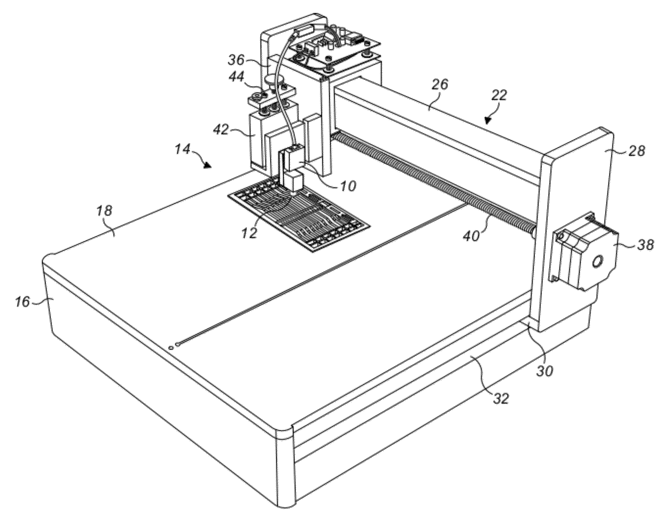
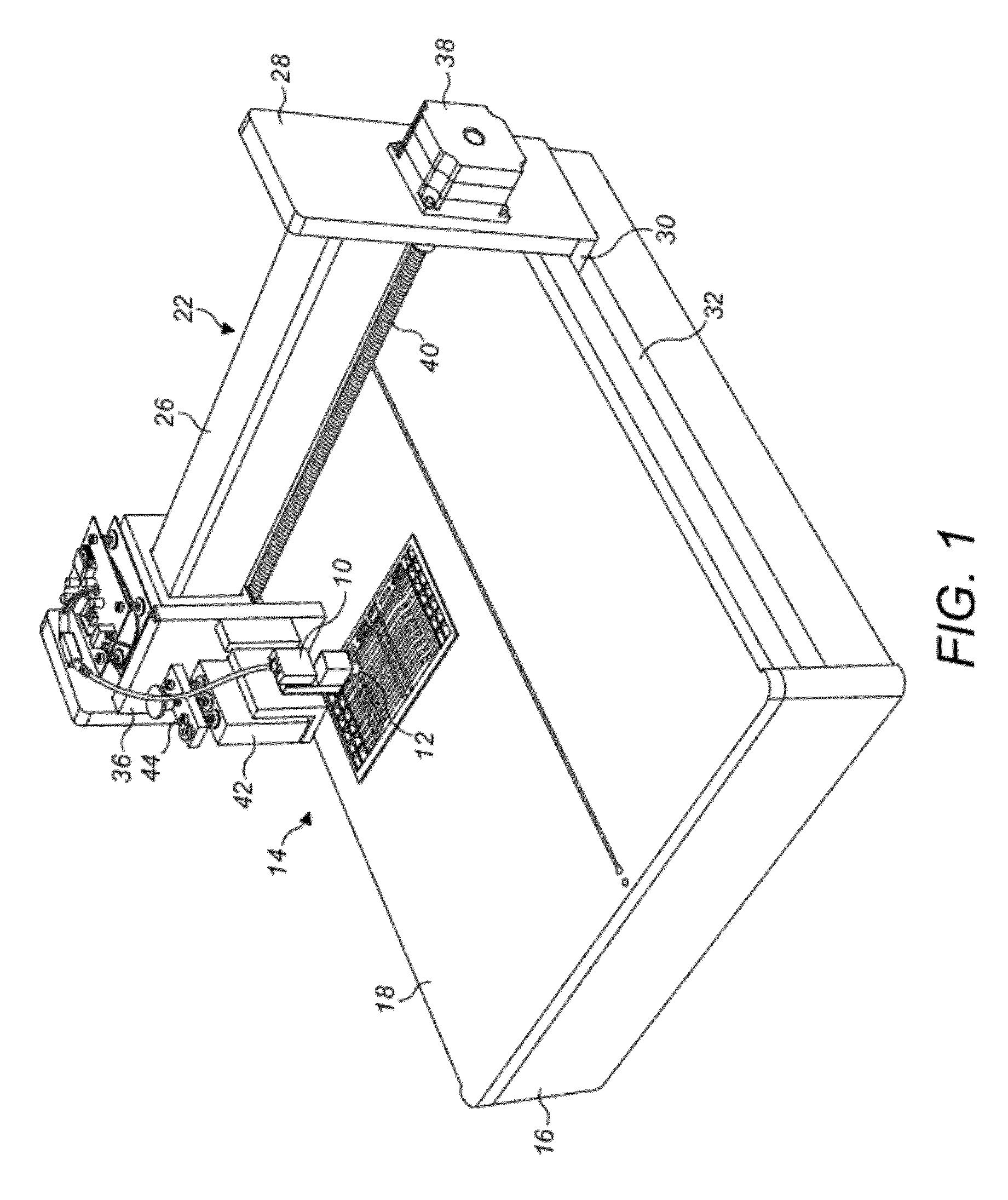
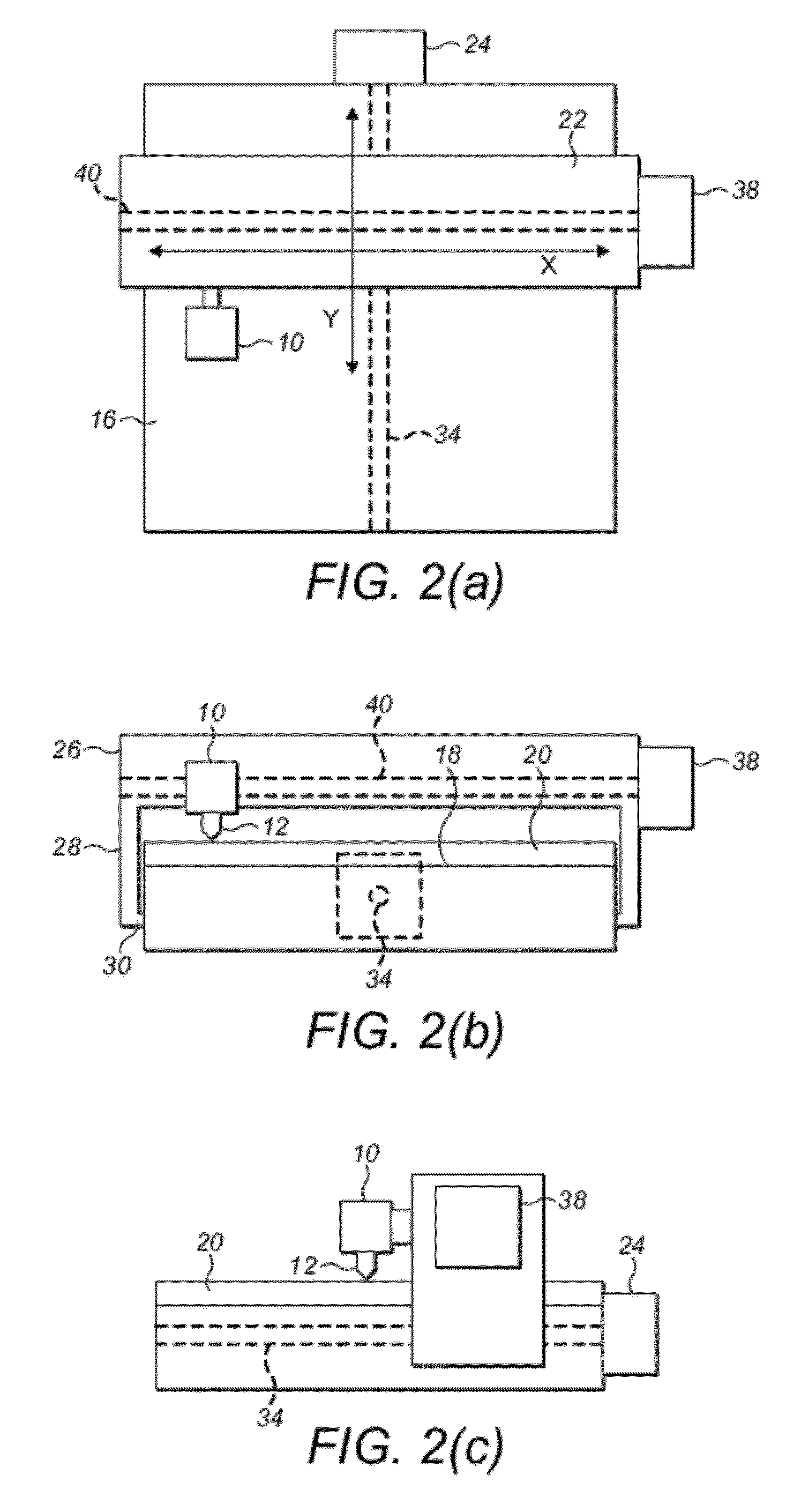
[0036]Referring initially to FIGS. 1 to 7, an embodiment of fingerprint detection apparatus according to the invention comprises a single electric potential sensor 10, a coaxial sensing probe 12 and a 3-axis positioning system 14, as shown.

[0037]The positioning system 14 comprises a flatbed support 16 having a horizontal plate surface 18 on which a sheet 20 of material, such as an insulating material, bearing a fingerprint may be placed. The electrical potential sensor 10 is mounted above the plate surface 18 to support the coaxial sensing probe 12 at a constant height above the plate surface 18 for scanning movement in the X-Y direction over the sheet 20. For this purpose, a gantry 22 is mounted on the base 16 for displacement in the Y direction along the full length of the plate 18 under the control of a stepper motor 24. The gantry 22 comprises a cross bar 26 extending between a pair of end plates 28 mounted on drive plates 30 located in linear slide bearing rails 32 on each side...


PUM


Abstract

The invention provides a method and apparatus for the detection of charge density distribution at the surface of a material sample. The apparatus comprises an electric potential sensor for measuring surface charge on a material sample, wherein the electrical potential sensor includes a probe for capacitively coupling the electric potential sensor to the surface of the material sample, an amplifier for generating a measurement output, the probe being connected to an input of the amplifier and the measurement output being supplied at an output of the amplifier, and a feedback arrangement driven from the output of the amplifier for enhancing the input impedance of the amplifier. A positioning system mounts the probe of the electric potential sensor above the material sample and moves the probe at a constant height over a surface of the said sample, and a processing system receives and processes the measurement output of the electric potential sensor for generating a digital record of the charge density distribution at the surface of the material sample.

Description

FIELD OF THE INVENTION[0001]The invention concerns apparatus and a method for measuring charge density distribution, and particularly apparatus and a method for measuring such charge density distribution resulting from fingerprints.BACKGROUND OF THE INVENTION[0002]Classic fingerprint evidence remains a primary forensic method of identification in many criminal cases. Techniques are known for detecting fingerprints on a variety of materials, but they generally rely on either visible deposits or hidden (latent) fingerprints resulting from the transfer of residues from the finger to the surface.[0003]Microscopic imaging techniques for this purpose suffer from severe limitations of scan area and scan speed. For example, atomic force microscopy can discern fingerprint residue on glass, but the scan area is restricted to 40 μm×40 μm, insufficient to image a whole fingerprint. Scanning electrochemical microscopy has a somewhat larger, but still restricted, scan area of 5 mm×3 mm; however, ...

Claims


Application Information

Patent Timeline
Patent Type & Authority Applications(United States)
IPC IPC(8): G06F19/00
CPCG06K9/0002G06V40/1306
Inventor PRANCE, HELENPRANCE, ROBERT JOHNWATSON, PHILIP
Owner THE UNIV OF SUSSEX
Why Eureka
Try Eureka