Photoelectric conversion device, light detecting device, and light detecting method

a conversion device and light detection technology, applied in the field of photoelectric conversion devices, can solve the problems of not being highly efficient in energy conversion and the logical limit of photoelectric conversion efficiency of silicon solar cells, and achieve the effect of high photoelectric conversion efficiency and simple manufacturing process

Active Publication Date: 2012-12-27
HOKKAIDO UNIVERSITY
View PDF4 Cites 18 Cited by
  • Summary
  • Abstract
  • Description
  • Claims
  • Application Information

AI Technical Summary

Benefits of technology

[0027]According to the present invention, it is possible to provide a photoelectric conversion device which can be manufactured through a simple manufacturing process, achieve photoelectric ...

Problems solved by technology

Photoelectric conversion efficiency of a silicon solar cell has a logical li...

Method used


Image

  • Photoelectric conversion device, light detecting device, and light detecting method
  • Photoelectric conversion device, light detecting device, and light detecting method
  • Photoelectric conversion device, light detecting device, and light detecting method

Examples


Embodiment Construction

[0046]Hereinafter, detailed descriptions will be provided on the preferable embodiments of a photoelectric conversion device and a photodetection device including the same according to the present invention with reference to the drawings. Like reference numerals designate identical or corresponding components throughout descriptions of the drawings, and duplicated descriptions thereof will be omitted. Each drawing has been made for the sake of the explanations, in which target parts of the explanations are described in an emphasizing manner. Therefore, the size proportion of each member in the drawings is not always corresponding to that of the actual one.

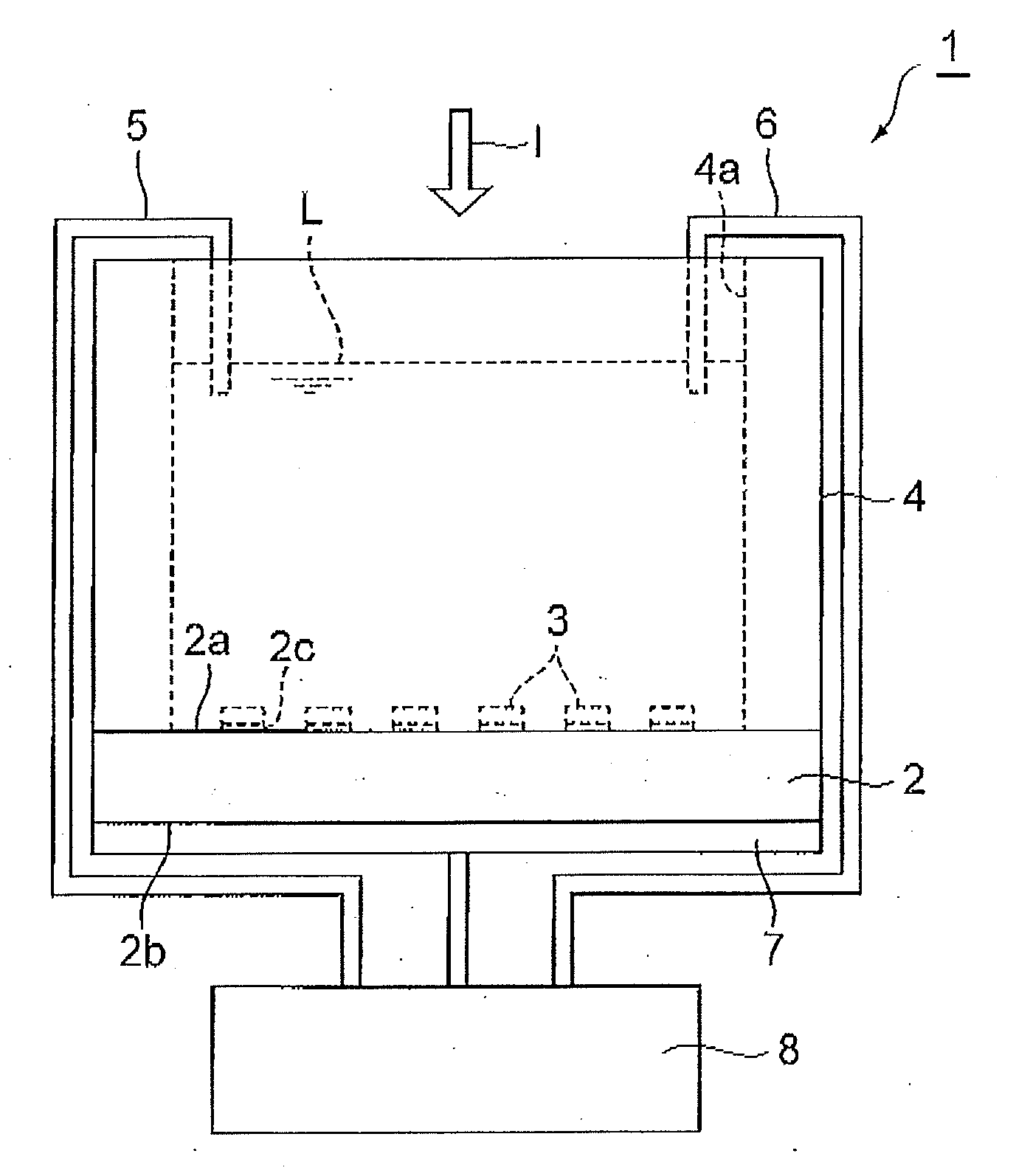
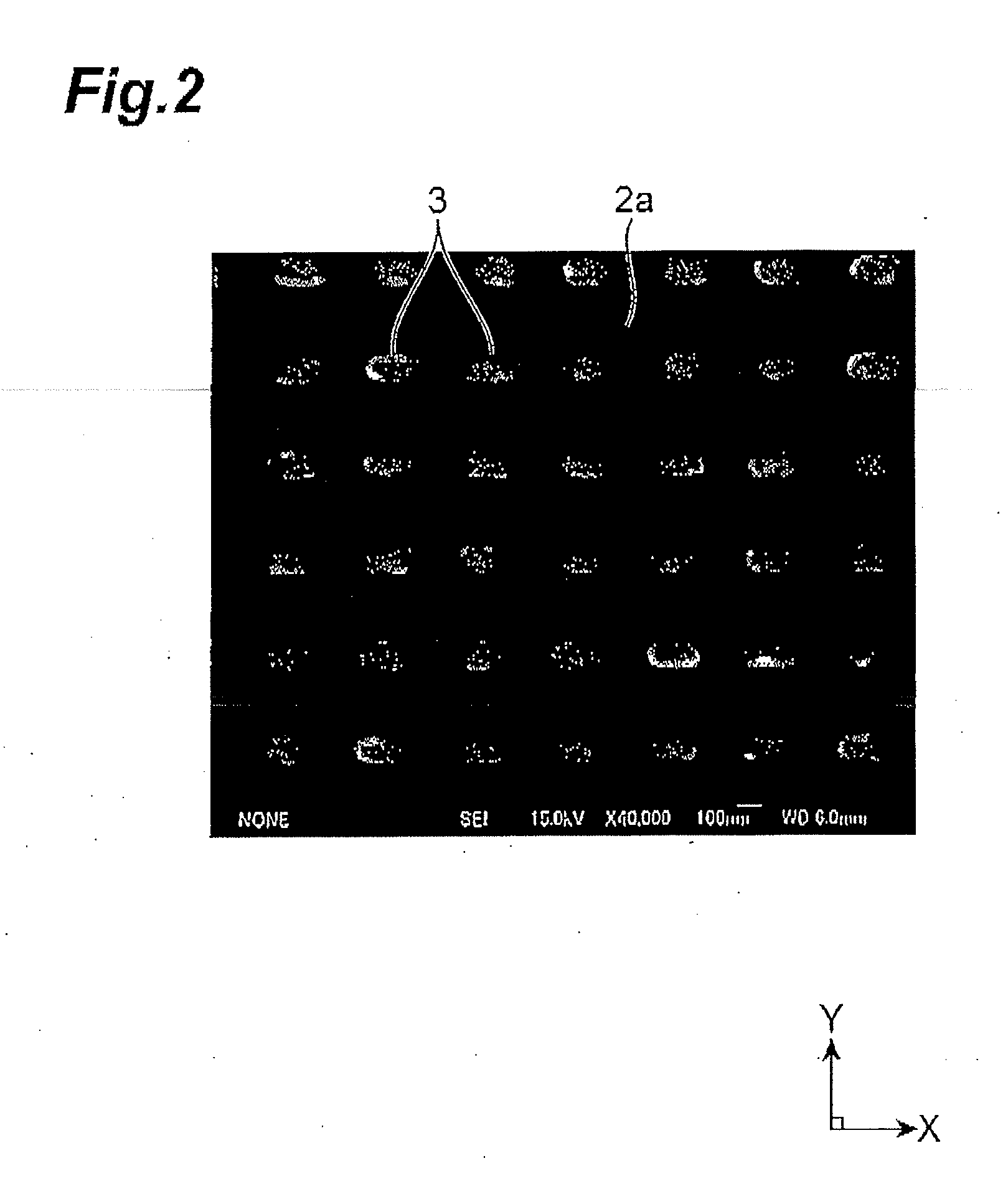
[0047]FIG. 1 is a front view of a photoelectric conversion device 1 according to one preferred embodiment of the present invention. This photoelectric conversion device 1 is a photoelectric conversion system for utilizing a metal microstructure functioning as an optical antenna that collects incident lights having various wavelengt...


PUM


Abstract

The present invention has an object to provide a photoelectric conversion device which can be manufactured through a simple manufacturing process, achieve photoelectric conversion over a wide range of wavelength regions, and attain high photoelectric conversion efficiency even in the infrared wavelength region, a photodetection device, and a photodetection method. This photoelectric conversion device 1 includes a substrate 2 containing single crystalline titanium dioxide, adhesion layers 2c formed on a surface 2a of the substrate 2, metal microstructure bodies 3, each of which has a volume of 1,000 nm3 or more and 3,000,000 nm3 or less, arranged at predetermined intervals in a predetermined direction on surfaces of the adhesion layers 2c, a container 4 for containing an electrolyte solution L in an arrangement region of the metal microstructure bodies 3 on the surface 2a of the substrate 2, a conductive layer 7 formed on a rear surface 2b of the substrate 2, and a counter electrode 5 in contact with the electrolyte solution L in the container 4; and the metal microstructure bodies 3 adhere onto the substrate 2 through the adhesion layers 2c, a Schottky barrier is formed at an interface of the substrate 2 with the metal microstructure bodies 3, and photoelectric conversion is carried out for light in an infrared region by utilizing a plasmon resonance phenomenon.

Description

TECHNICAL FIELD[0001]The present invention relates to a photoelectric conversion device, a photodetection device, and a photodetection method.BACKGROUND ART[0002]Currently, a silicon solar cell is widely utilized as one kind of photoelectric conversion device. Photoelectric conversion efficiency of a silicon solar cell has a logical limit of approximately 30%, and this is not such highly efficient energy conversion. This results from the following reasons: (i) near-infrared light whose wavelength is longer than a band edge of silicon (equivalent to wavelength of 1100 nm) does not contribute to photoelectric conversion, (ii) light whose wavelength is shorter than 1100 nm, although absorbed by silicon, is mostly not utilized in photoelectric conversion but converted into heat because of energy relaxation. In order to address the above two problems, it is required to create a photoelectric conversion system that realizes effective utilization of energy in all wavelength regions of the ...

Claims


Application Information

Patent Timeline
IPC IPC(8): H01L31/07
CPCH01G9/2031Y02E10/542H01G9/2022Y02P70/50H01L29/47H01L31/022425H01L31/18
Inventor MISAWA, HIROAKINISHIJIMA, YOSHIAKIUENO, KOSEIMURAKOSHI, KEI
Owner HOKKAIDO UNIVERSITY
Why Eureka
Try Eureka