Nanoscale interconnects fabricated by electrical field directed assembly of nanoelements

a technology of electrical field and nanoelement, which is applied in the direction of liquid/fluent solid measurement, fluid pressure measurement, peptide, etc., can solve the problems of process providing no control over the length of nanorods, unsuitable specific application of fabrication techniques, etc., and achieve the effect of controlling the directed assembly process

Active Publication Date: 2012-12-27
NORTHEASTERN UNIV
View PDF3 Cites 19 Cited by
  • Summary
  • Abstract
  • Description
  • Claims
  • Application Information

AI Technical Summary

Benefits of technology

[0008]The invention provides methods for fabricating electrically conductive nanorods or interconnects using electric-field-directed assembly of nanoparticles or nanotubes and interconnects made by the methods. An externally applied dynamic electric field (AC) with a DC offset allows nanoparticles such as colloidal gold to uniformly assemble and fuse in prepatterned surfaces (vias). The electric field is applied between a prepatterned surface containing vias and a counter electrode placed 5 mm away from the vias. Control over the directed-assembly process is provided by manipulation of different forces acting on the nanoparticles or nanotubes imposed by AC and DC electric fields. The assembly process is carried out in aqueous solution having a pH greater than 7, e.g., with a low concentration of ammonium hydroxide and hence is environmentally green. The fabricated nanorods can be used for various nanoscale applications including electronic, photonic, and biomedical devices.

Problems solved by technology

In these assembly processes, the two electrodes required for applying the electric field are usually on the same substrate or very close to each other (order of microns), making the fabrication techniques unsuitable for specific applications such as interconnects in CMOS-based devices [19] and various types of electromagnetic-field-enhancement sensors.
However, the process provided no control over the length of the nanorods, impeding the potential use of the rods in sensors and CMOS interconnect applications.
However, these high temperature processes are not compatible with CMOS technology [14, 15].
For local vertical interconnects, the methods that have been carried out are not highly scalable.

Method used


Image

  • Nanoscale interconnects fabricated by electrical field directed assembly of nanoelements
  • Nanoscale interconnects fabricated by electrical field directed assembly of nanoelements
  • Nanoscale interconnects fabricated by electrical field directed assembly of nanoelements

Examples


example 1

Materials and Methods

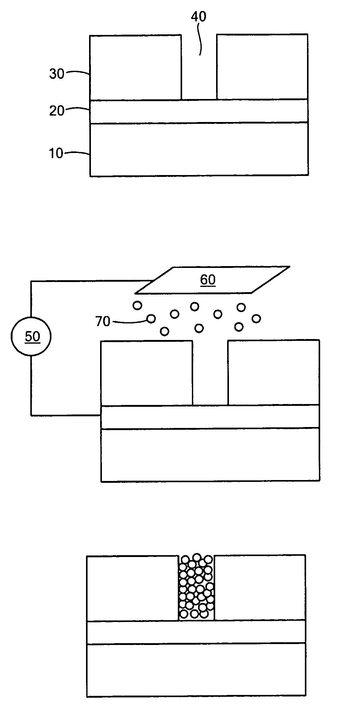
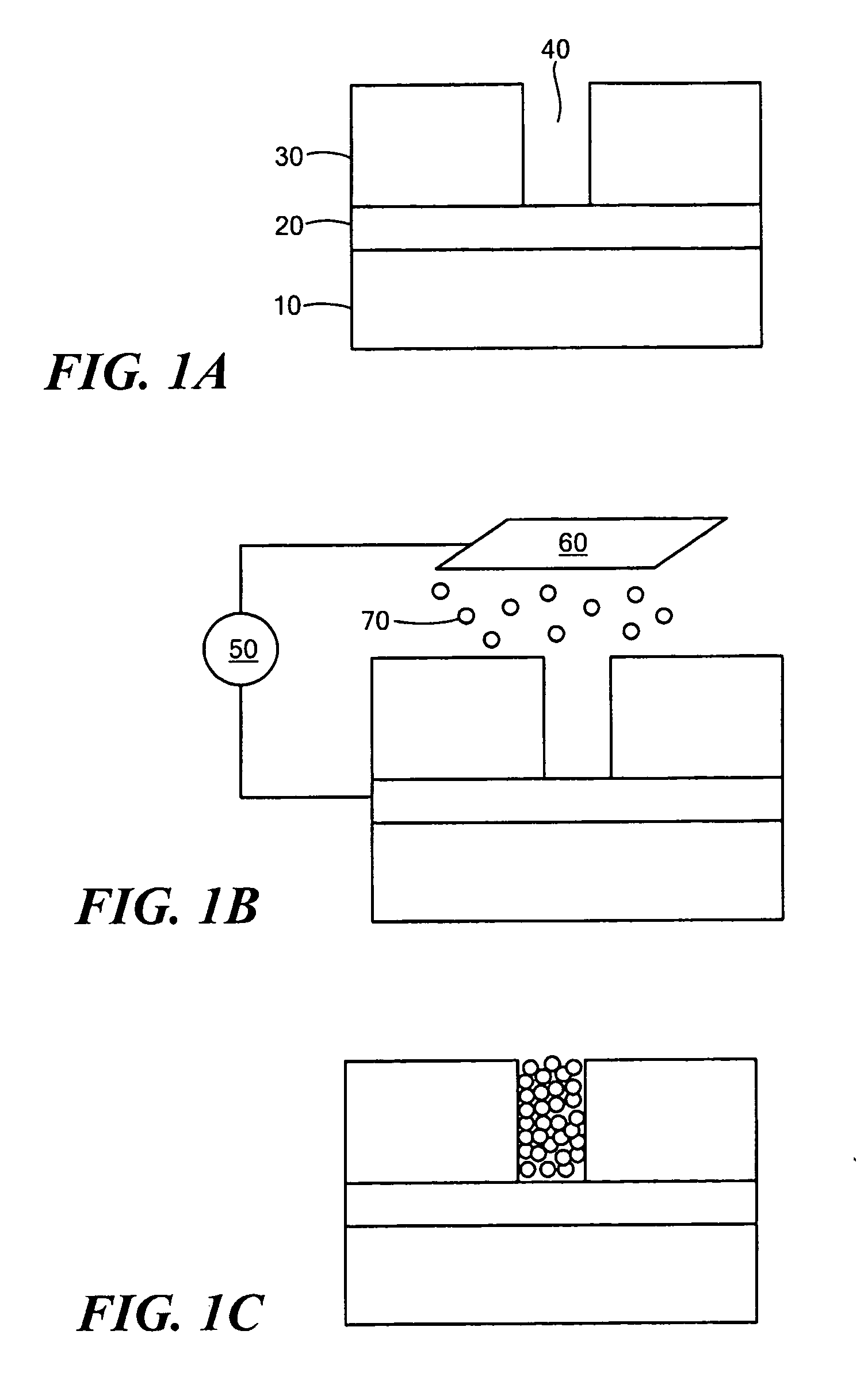
[0043]The following materials and methods were used in the Examples which follow. Gold nanoparticles (50 nm in diameter) supplied by Ted Pella Corporation were used in the assembly. The concentration of the particles in the aqueous suspension was 4.5×10¹⁰ particles / cm3. The zeta potential of the nanoparticles was measured using a Malvern Zeta Plus 90 zeta-potentiometer. To create nanoscale vias shown in FIG. 1(a), Cr / Au (2 nm Cr / 120 nm Au) was sputtered on SiO2 / Si (470 nm layer of SiO2 on 380 μm thick Si) wafer and then diced into 12 mm x 12 mm chips. Positive photoresist (poly-methyl-methacrylate (PMMA)) was spin-coated on the precleaned Cr / Au chips (precleaning with Piranha solution, H2SO4 / H2O2, 2 / 1 vol / vol). The nanoscale via array was fabricated (in PMMA) using conventional electron-beam lithography. In total, 256 vias were patterned over a 40 μm×40 μm area. The via dimensions were in the range of 100-150 nm in depth, and 100-500 nm in diameter with separati...

example 2

Electric Field-Directed Assembly of Nanorods from Gold Nanoparticles

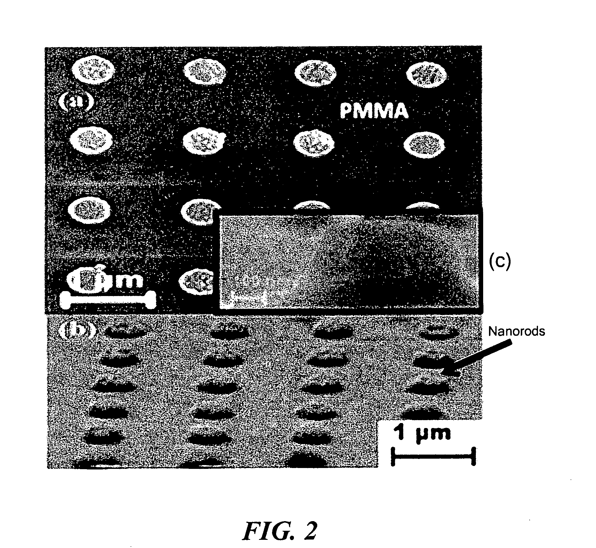
[0044]FIGS. 2(a) and 2(b) show top-down and high-angle-viewed scanning electron micrographs (SEMs) of an array of vias each 500-nm in diameter and 150-nm deep after electric-field directed assembly of 50-nm gold nanoparticles. An AC voltage of 12 Vpp (where pp denotes peak-to-peak) with a frequency of 10 kHz and a DC offset of 2 V was applied for 90 s during the assembly process. The SEM image of FIG. 2(b) also shows that the height of the produced nanorods is uniform over the array and exceeds the PMMA surface. An atomic force microscopy (AFM) scan of a 5 μm×5 μm area using a PSIA XE150 atomic force microscope is shown in FIG. 3. While the lateral dimensions of the nanorods were influenced by AFM tip effects, the vertical dimensions were in the range of 90-125 nm. By taking the 150-nm PMMA thickness into account, the results over 16 nanorods showed that the height varied between 240 nm (min) and 275 nm (max) with a...

example 3

Effects of Electric Field Parameters on Nanoparticle Assembly

[0045]The effects of various parameters of the applied electric field on the nature of assembly were investigated. The behavior of nanoparticle assemblies in the vias under influence of individually applied DC and AC voltages was studied separately. FIG. 4 shows a topdown-viewed SEM after assembly was carried out by employing a uniform (DC) voltage of 2V for 90 s. Only a few particles were assembled in the vias. The induced charge on the 50-nm gold nanoparticles (measured zeta potential of −55 mV) is estimated to be O(10−17) C. Using Stokes' law, the particles were estimated to reach a terminal velocity of ˜30 μm / s at an applied voltage of 2 V. Although the velocity of the particles was sufficient to reach the template surface, most of the regions in the vias remained empty without having nanoparticle assembly.

[0046]In order to test a dynamic electric field (AC) only, the voltage was set to 12 Vpp with a frequency of 10 kH...


PUM

PropertyMeasurementUnit
steady-state currentaaaaaaaaaa
DC voltageaaaaaaaaaa
AC voltageaaaaaaaaaa

Abstract

The invention provides a fast, scalable, room temperature process for fabricating metallic nanorods from nanoparticles or fabricating metallic or semiconducting nanorods from carbon nanotubes suspended in an aqueous solution. The assembled nanorods are suitable for use as nanoscale interconnects in CMOS-based devices and sensors. Metallic nanoparticles or carbon nanotubes are assembled into lithographically patterned vias by applying an external electric field. Since the dimensions of nanorods are controlled by the dimensions of vias, the nanorod dimensions can be scaled down to the low nanometer range. The aqueous assembly process is environmentally friendly and can be used to make nanorods using different types of metallic particles as well as semiconducting and metallic nanaotubes.

Description

CROSS REFERENCE TO RELATED APPLICATIONS[0001]Priority is claimed to U.S. Provisional Application Ser. No. 61 / 247,706, entitled “Nano-particle Interconnects by Directed Assembly”, filed on Oct. 1, 2009, and to U.S. Provisional Application Ser. No. 61 / 248,929, entitled “Single Wall Carbon Nanotube Interconnects by Directed Assembly”, filed on Oct. 6, 2009. Both of said provisional applications are hereby incorporated by reference in their entireties.STATEMENT REGARDING FEDERALLY SPONSORED RESEARCH OR DEVELOPMENT[0002]The invention was developed with financial support by Grant No. 0425826 from the National Science Foundation. The U.S. Government has certain rights in the invention.BACKGROUND[0003]The precise assembly of nanoscale materials in a desired location and orientation on surfaces makes possible the fabrication of various types of novel structures and devices [1]-[3]. Nanoparticles are model nanoscale building blocks due to their zero-dimensional geometry and unique size-depend...

Claims


Application Information

Patent Timeline
Patent Type & Authority Applications(United States)
IPC IPC(8): C25B15/00C25B11/02H01L23/482B82Y40/00B82Y99/00
CPCB82Y10/00B82Y30/00H01L21/2885H01L21/76879H01L23/53242H01L2924/0002H01L23/53276H01L2221/1094H01L2924/00C25D13/00H01L23/5226H01L23/53214H01L23/53228H01L23/53257
Inventor BUSNAINA, AHMEDYILMAZ, CIHANKIM, TAEHOONSOMU, SIVASUBRAMANIAN
Owner NORTHEASTERN UNIV
Why Eureka
Try Eureka