Charged Particle Beam Microscope

Active Publication Date: 2012-12-27
HITACHI HIGH-TECH CORP
View PDF41 Cites 1 Cited by
  • Summary
  • Abstract
  • Description
  • Claims
  • Application Information

AI Technical Summary

Benefits of technology

[0018]It is possible to provide a charged particle beam microscope which can obtain information about the materials and stereostructure of a patte

Problems solved by technology

Photoresist for an ArF (wavelength 193 nm) exposure apparatus which has been used recently in the fabrication of semiconductor devices has a problem that it is damaged by electron beam irradiation, resulting in volume shrinkage.
For a semiconductor device to demonstrate performance as desig

Method used


Image

  • Charged Particle Beam Microscope
  • Charged Particle Beam Microscope
  • Charged Particle Beam Microscope

Examples


first embodiment

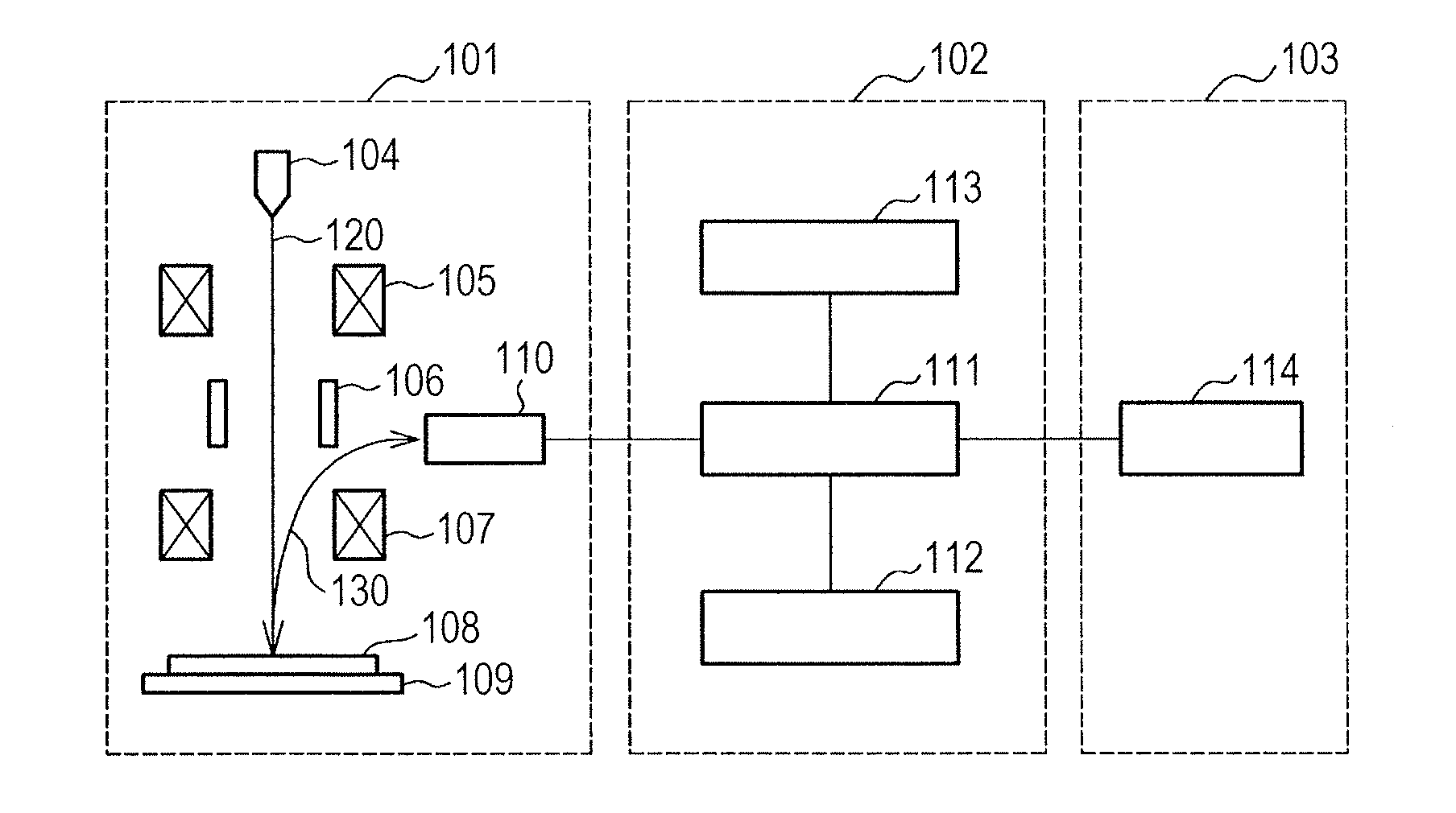
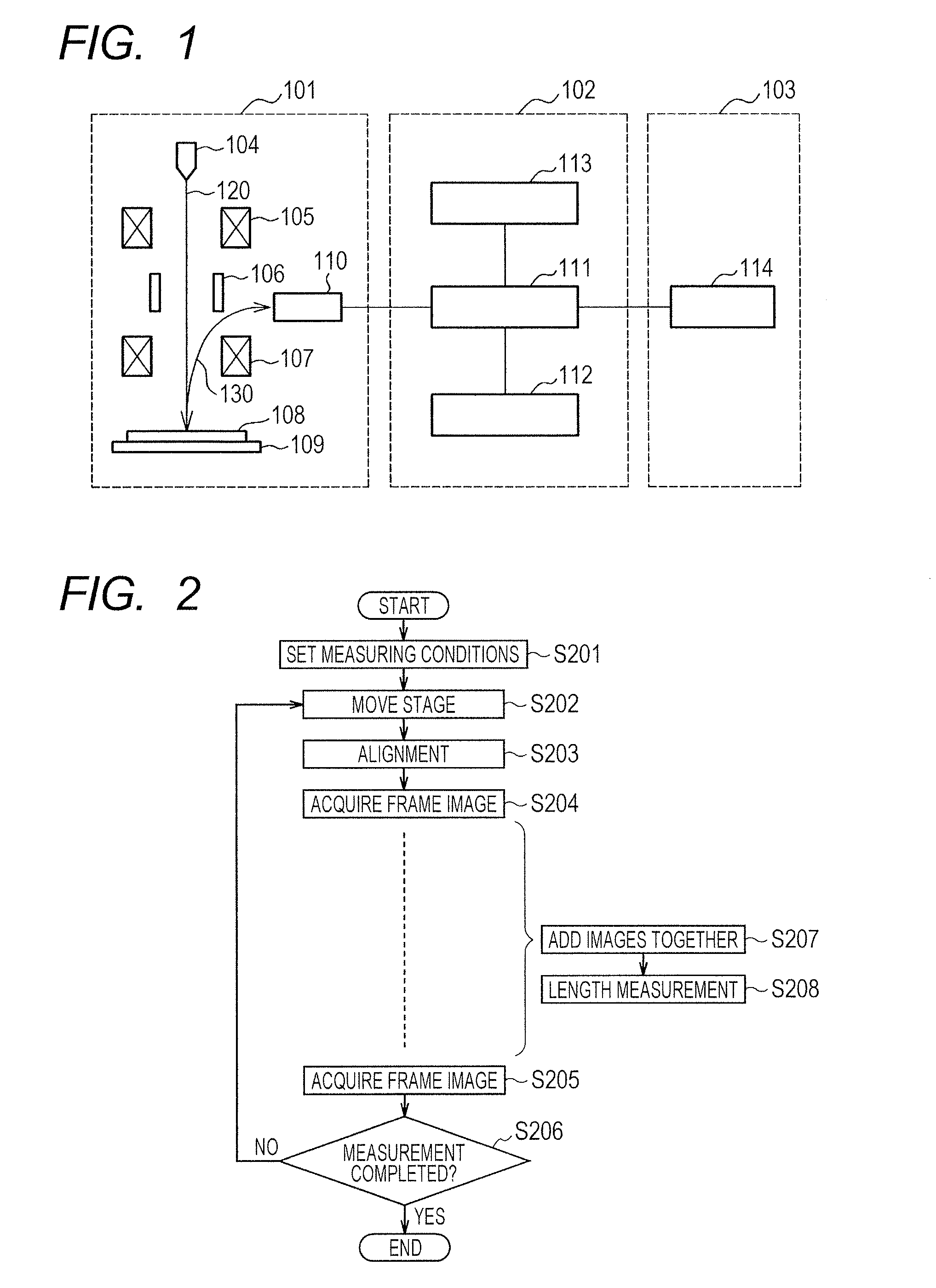
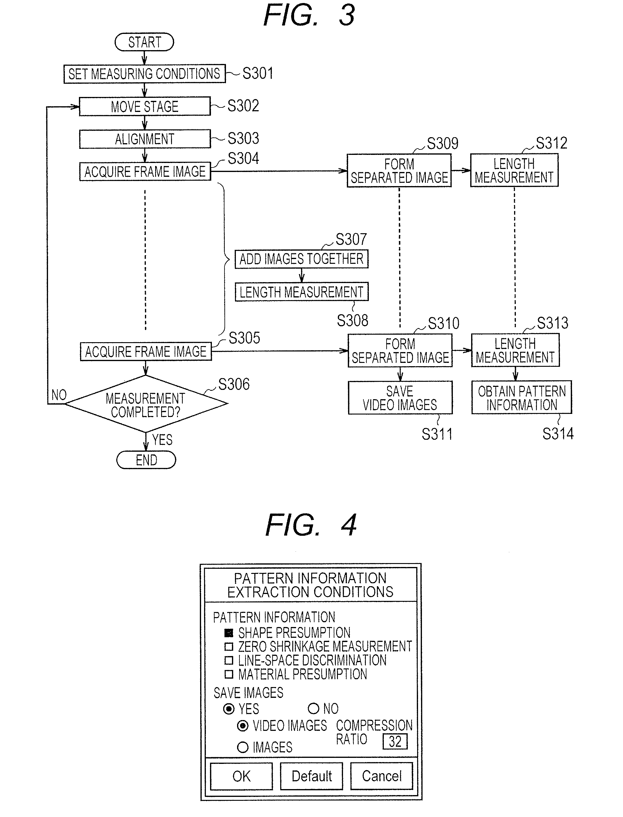
[0037]A first embodiment will be described referring to FIG. 1 to FIG. 8. FIG. 1 is a view showing the configuration of a scanning electron microscope according to this embodiment. This device has a function to make an image for length measurement by adding together frame images and measure lengths and makes it possible to obtain pattern information from change over time of plural frame images constituting the image for length measurement. Here, an image made by adding together plural frame images acquired by scanning the field of view once is defined as an image for length measurement.

[0038]The scanning electron microscope with a function to obtain pattern information includes an electron microscope unit 101, a control unit 102, and a display unit 103. An electron beam 120 emitted from an electron source 104 is converged by a condenser lens 105 and an objective lens 107 and then thrown on a sample 108 placed on a sample stage 109. The electron beam is scanned over the sample two-di...

second embodiment

[0068]A second embodiment will be described referring to FIG. 9 and FIG. 10. What has been described about the first embodiment is also applicable to this embodiment unless there are special circumstances. In this embodiment, zero shrinkage presumption will be explained.

[0069]FIG. 9 show a method of measuring dimensions before shrinkage by comparison with the conventional method. FIG. 9A shows the conventional method of calculating zero time values and FIG. 9B shows the method according to the present invention.

[0070]First, FIG. 9A is explained. The process of acquiring an image for length measurement by scanning the spot to be observed more than once is first carried out more than once and the length measurement value of each image for length measurement is calculated. The length measurement value is plotted on the vertical axis versus the number of measurements on the horizontal axis. Since the resist pattern tends to have a characteristic that it shrinks due to electron beam irra...

third embodiment

[0082]A third embodiment will be described referring to FIG. 12 and FIG. 13. What has been described about the first embodiment is also applicable to this embodiment unless there are special circumstances. In this embodiment, an explanation is given of a technique of deciding whether for a resist pattern it is a pattern to remain intact (Line pattern) or a portion to be lost (Space pattern).

[0083]FIG. 12A shows an example of an image of a pattern being observed. Shown here is an example that no difference in shading contrast is seen between the Line portions and Space portions. Not only in this case, this technique can be applied in a case that shading is seen but discrimination between patterns to remain intact and portions to be lost is impossible or a case that the shading contrast of a pattern changes during observation. In order to address this problem, in this embodiment, length measurement values of neighboring pattern widths CD1 and CD2 are measured.

[0084]FIG. 12B shows the ...


PUM


Abstract

Disclosed is a charged particle beam microscope which can obtain information about pattern materials and stereostructure without lowering throughput of pattern dimension measurement. To achieve this, the charged particle beam microscope acquires a plurality of frame images by scanning the field of view of the sample (S304, 305), adds the images together (S307), computes the dimensions of the pattern formed on the sample (308) and at the same time acquires pattern information (314) using components of a frame image, such as a single frame image or subframe image, as a separated image (309, 310).

Description

TECHNICAL FIELD[0001]The present invention relates to a charged particle beam microscope and more particularly to a charged particle beam microscope including a scanning electron microscope for measuring a sample as a measuring object which may change in shape or be charged by electron beam irradiation.BACKGROUND ART[0002]A charged particle beam microscope, for example, a scanning electron microscope, is an instrument which irradiates a sample with a narrow electron beam, detects secondary electrons or reflected electrons generated by electron beam irradiation, and modulates the brightness according to the detection signal to form an image.[0003]In the semiconductor manufacturing process, with the trend toward finer patterns, there is demand for an instrument which provides high measurement accuracy. As a dimension measuring tool for measuring the widths of fine patterns on the order of dozens of nanometers which can not be measured by an optical measuring instrument, a scanning ele...

Claims


Application Information

Patent Timeline
IPC IPC(8): H04N7/18
CPCG01B15/00H01J37/28H01J2237/221H01J2237/24578G01B15/04H01J2237/2067H01J2237/2817
Inventor OKAI, NOBUHIROSOHDA, YASUNARITANAKA, JUNICHI
Owner HITACHI HIGH-TECH CORP
Why Eureka
Try Eureka