Laminated high melting point soldering layer and fabrication method for the same, and semiconductor device

a high melting point and soldering layer technology, applied in the direction of manufacturing tools, solvents, transportation and packaging, etc., can solve the problems of inability to use sic devices, inability to drive at high temperature, and spoiled reliability of sic devices, so as to shorten the process time duration, increase mass production volume efficiency, and high melting point

Active Publication Date: 2013-01-03
ROHM CO LTD
View PDF4 Cites 36 Cited by
  • Summary
  • Abstract
  • Description
  • Claims
  • Application Information

AI Technical Summary

Benefits of technology

[0024]According to the present invention, it can provide a laminated high melting point soldering layer and a fabrication method for such laminated high melting point soldering layer which can increase mass production volume efficiency by applying

Problems solved by technology

However, since the SiC devices can theoretically operate to about 400 degrees C., if the SiC devices are driven at high temperature when using the conventional low melting point solder, the short circuit between electrodes, the delamination between the SiC devices and a base plate, etc. occurred by fusing bonding parts when using the low melting point solder,

Method used


Image

  • Laminated high melting point soldering layer and fabrication method for the same, and semiconductor device
  • Laminated high melting point soldering layer and fabrication method for the same, and semiconductor device
  • Laminated high melting point soldering layer and fabrication method for the same, and semiconductor device

Examples


embodiment

Configuration of Laminated High Melting Point Soldering Layer

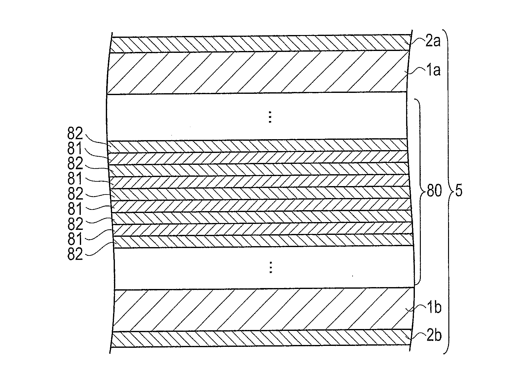
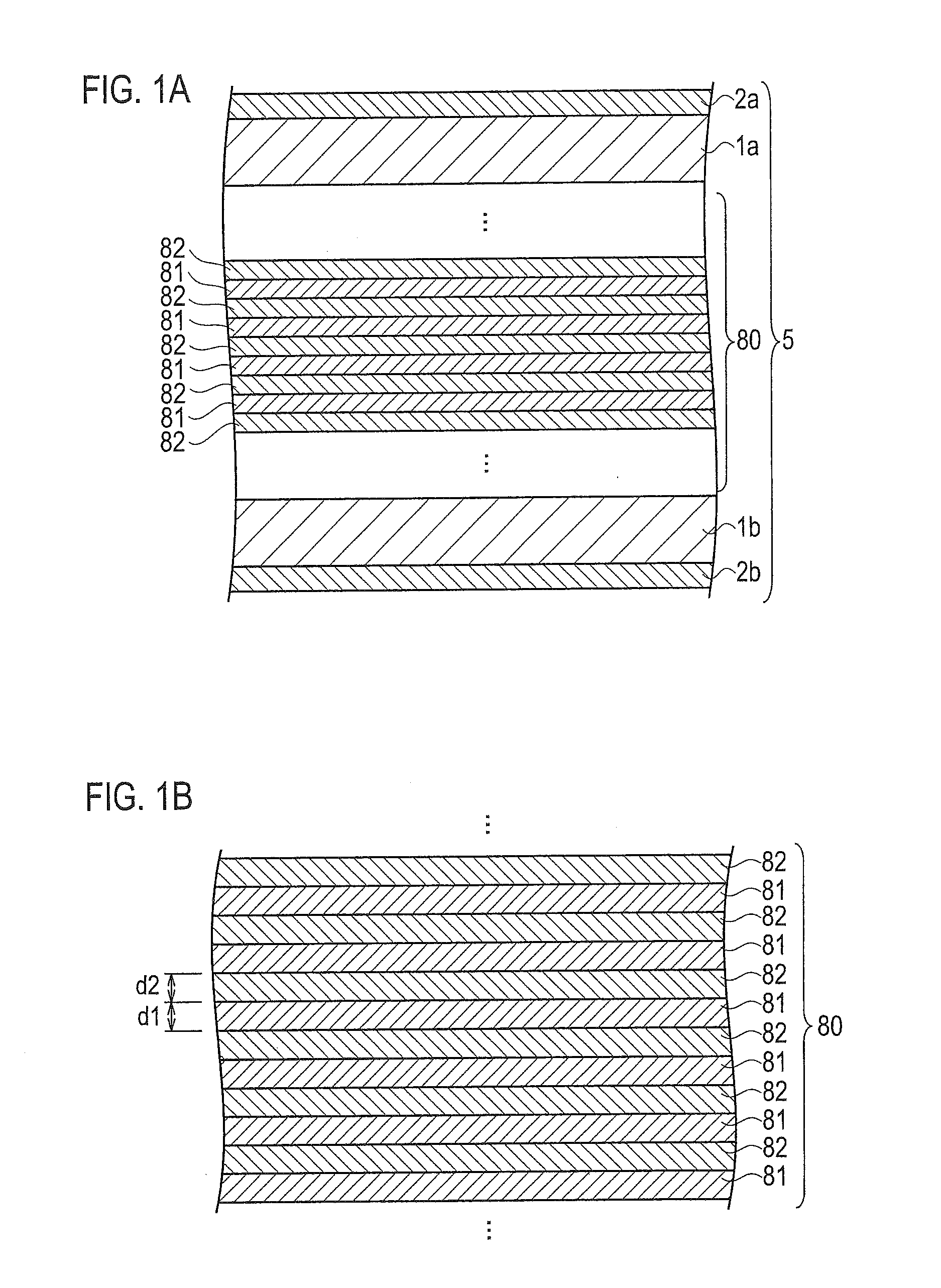
[0047]FIG. 1A is a schematic cross-sectional configuration diagram showing a laminated high melting point soldering layer 5 according to an embodiment, and FIG. 1B is a schematic cross-sectional configuration diagram of a laminated structure 80 which laminated a plurality of three-layered structures, the respective three-layered structures including a low melting point metal thin film layer 81, and high melting point metal thin film layers 82 disposed on the surface and back side surface of the low melting point metal thin film layer 81.

[0048]As shown in FIG. 1A and FIG. 1B, the laminated high melting point soldering layer 5 according to the embodiment includes: the laminated structure 80 which laminated the plurality of the three-layered structures, the respective three-layered structures including the low melting point metal thin film layer 81, and the high melting point metal thin film layers 82 disposed on the surface ...

modified example

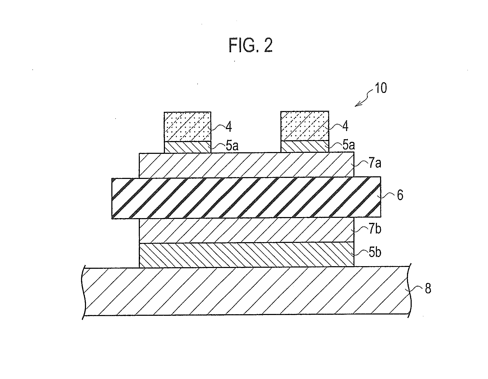
[0102]As shown in FIGS. 17A and 17B, a semiconductor device 10 according to a modified example to which the laminated high melting point soldering layer according to the embodiment is applied includes: a semiconductor device 4; a third laminated high melting point soldering layer 5c disposed on the semiconductor device 4; a source side pad electrode 40 disposed on the third laminated high melting point soldering layer 5c; a fourth laminated high melting point soldering layer 5d disposed on the back side surface of the semiconductor device 4 of the opposite side to the surface where the third laminated high melting point soldering layer 5c is disposed; and a drain side pad electrode 42 disposed on the backside surface of the fourth laminated high melting point soldering layer 5d of the opposite side to the surface of the fourth laminated high melting point soldering layer 5d where the semiconductor device 4 is disposed. In the semiconductor device 10 shown in FIG. 17, the three semic...


PUM

PropertyMeasurementUnit
Fractionaaaaaaaaaa
Fractionaaaaaaaaaa
Fractionaaaaaaaaaa

Abstract

The laminated high melting point soldering layer includes: a laminated structure which laminated a plurality of three-layered structures, the respective three-layered structures including a low melting point metal thin film layer and a high melting point metal thin film layers disposed on a surface and a back side surface of the low melting point metal thin film layer; a first high melting point metal layer disposed on the surface of the laminated structure; and a second high melting point metal layer disposed on the back side surface of the laminated structure. The low melting point metal thin film layer and the high melting point metal thin film layer are mutually alloyed by TLP, and the laminated structure, and the first high melting point metal layer and the second high melting point metal layer are mutually alloyed by the TLP bonding.

Description

TECHNICAL FIELD[0001]The present invention relates to a laminated high melting point soldering layer, a fabrication method for such high melting point soldering layer, and a semiconductor device. More specifically, the present invention relates to a laminated high melting point soldering layer fabricated by TLP (Transient Liquid Phase) bonding, a fabrication method for such high melting point soldering layer, and a semiconductor device.BACKGROUND ART[0002]Currently, research and development of an SiC (Silicon Carbide) device are done in many research institutions. As a characteristic of the SiC devices, it can be mentioned of low on resistance, high speed switching, high temperature operation, etc.[0003]Conventionally, since the temperature span which can operate in Si devices, such as IGBTs (Insulated Gate Bipolar Transistors), currently used in the field of a semiconductor power module is to about 150 degrees C., it was possible to have driven even when using low melting point sol...

Claims


Application Information

Patent Timeline
IPC IPC(8): H01L23/532H01L23/485B32B15/01B23K1/20B23K35/02
CPCB23K1/0016Y10T428/12986B23K35/262B23K35/3006B23K35/3033B23K20/023B23K35/007B23K35/0238H01L23/3735H01L23/4827H01L24/48B23K2201/40H01L2224/32225H01L2224/48227H01L2224/73265H01L2924/13091H01L2924/00014B23K1/20Y10T428/12715H01L2924/1305H01L2224/29155H01L2224/83101H01L2224/29139H01L2224/29111H01L2224/2908H01L24/83H01L24/32H01L24/27H01L2924/0132H01L2924/1461C22C13/00B32B15/018H01L24/29H01L2924/13055H01L2924/01322H01L2224/48091H01L2924/3511H01L2924/00012H01L2224/45099H01L2924/00H01L2924/01047H01L2924/0105B23K2101/40H01L24/73H01L2224/83825
Inventor OTSUKA, TAKUKAZUOKUMURA, KEIJI
Owner ROHM CO LTD
Why Eureka
Try Eureka