Methods for fabricating a finfet integrated circuit on a bulk silicon substrate

Inactive Publication Date: 2013-01-03
GLOBALFOUNDRIES US INC
View PDF3 Cites 194 Cited by
  • Summary
  • Abstract
  • Description
  • Claims
  • Application Information

AI Technical Summary

Benefits of technology

[0007]In accordance with another embodiment a method for fabricating a FINFET integrated circuit includes growing a silicon germanium epitaxial layer overlying a silicon substrate and growing a silicon epitaxial layer overlying the silicon germanium epitaxial layer. Shallow trench isolation is formed to define a device region. The silicon epitaxial layer is etched in an etchant that etches silicon at a substantially higher etch rate than the etch rate of silicon germanium to form a silicon fin extending across the device region and contacting t

Problems solved by technology

SOI substrates are expensive, however, so there are significant economic advantages to fabricating the ICs on bulk wafers.
A number of techniques have been attempted to provide isolation between fins of a bulk wafer FINFET IC, but such attempts have had limited success.
Among the disadvantages of such i

Method used


Image

  • Methods for fabricating a finfet integrated circuit on a bulk silicon substrate
  • Methods for fabricating a finfet integrated circuit on a bulk silicon substrate
  • Methods for fabricating a finfet integrated circuit on a bulk silicon substrate

Examples


Embodiment Construction

[0014]The following detailed description is merely exemplary in nature and is not intended to limit the invention or the application and uses of the invention. Furthermore, there is no intention to be bound by any expressed or implied theory presented in the preceding technical field, background, brief summary or the following detailed description.

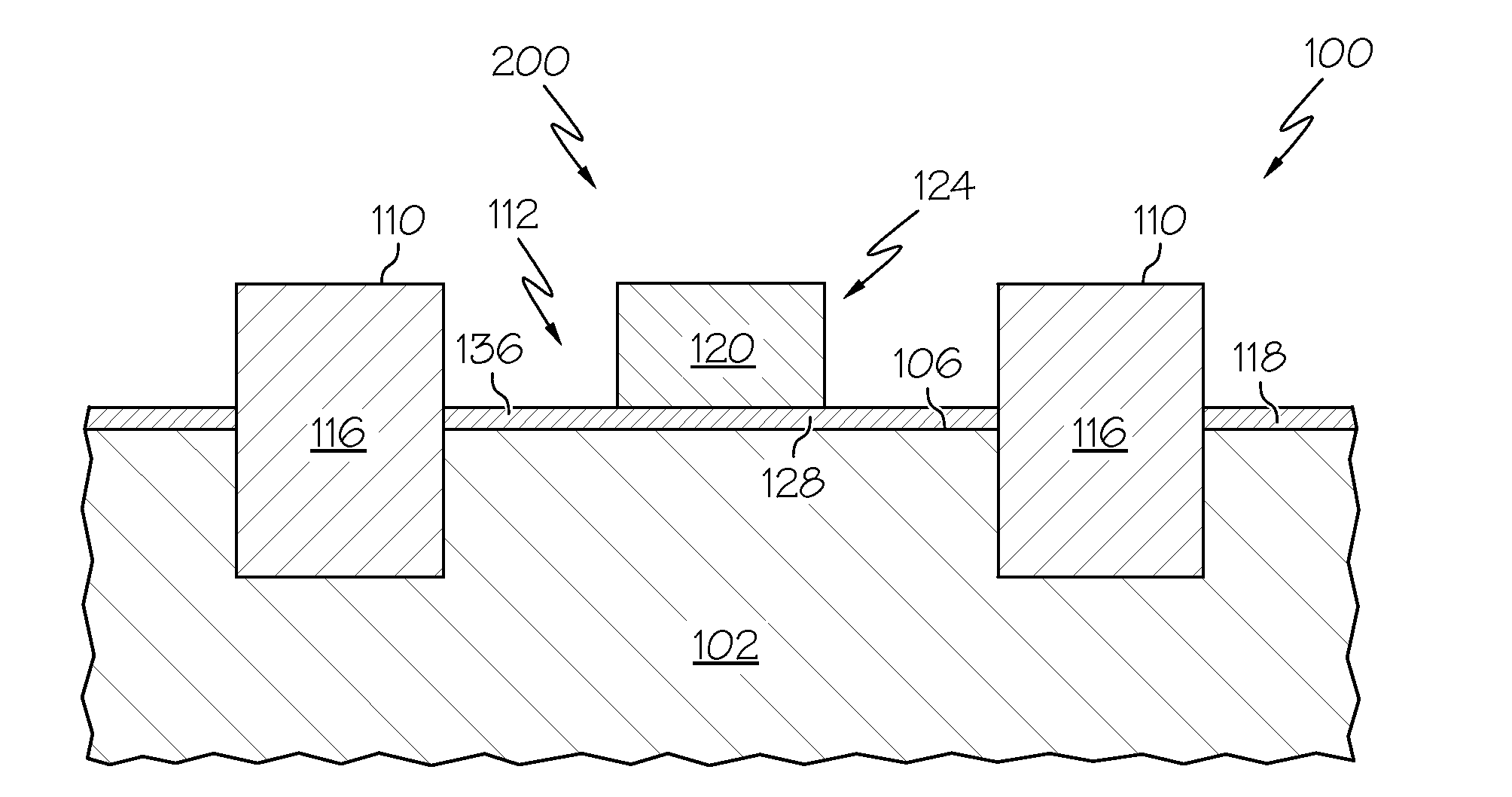
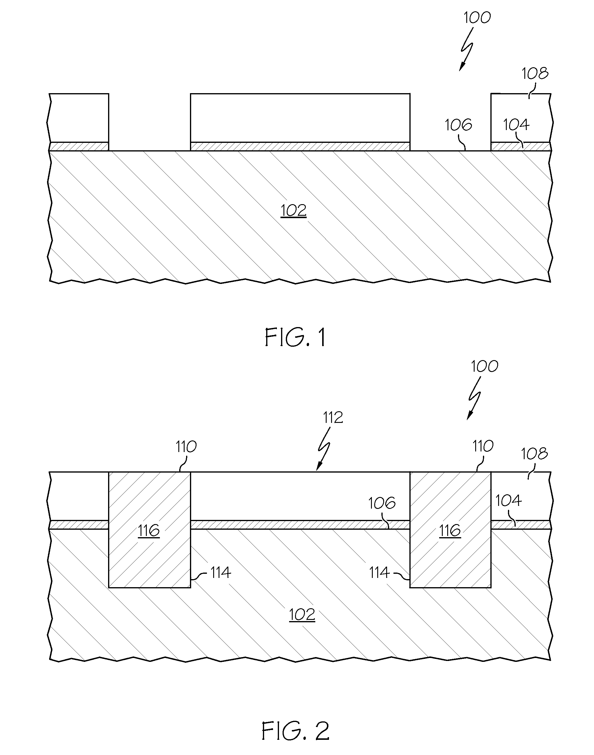
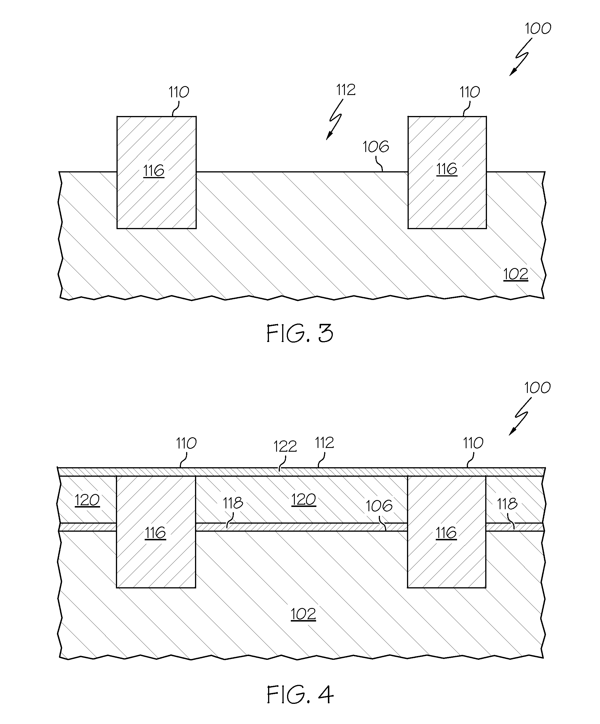
[0015]FIGS. 1-10 illustrate method steps for fabricating a FINFET integrated circuit (IC) 100 in accordance with various embodiments. The described process steps, procedures, and materials are to be considered only as exemplary embodiments designed to illustrate to one of ordinary skill in the art methods for practicing the invention; the invention is not to be limited to these exemplary embodiments. Various steps in the manufacture of ICs are well known and so, in the interest of brevity, many conventional steps will only be mentioned briefly herein or will be omitted entirely without providing the well known process details. The FIGURES ...


PUM


Abstract

Methods are provided for fabricating a FINFET integrated circuit that includes epitaxially growing a first silicon germanium layer and a second silicon layer overlying a silicon substrate. The second silicon layer is etched to form a silicon fin using the first silicon germanium layer as an etch stop. The first silicon germanium layer underlying the fin is removed to form a void underlying the fin and the void is filled with an insulating material. A gate structure is then formed overlying the fin.

Description

TECHNICAL FIELD[0001]The present invention generally relates to methods for manufacturing integrated circuits, and more particularly relates to methods for manufacturing FINFET integrated circuits on bulk silicon substrates.BACKGROUND[0002]Transistors such as metal oxide semiconductor field effect transistors (MOSFETs) or simply field effect transistors (FETs) or MOS transistors are the core building blocks of the vast majority of semiconductor integrated circuits (ICs). A FET includes source and drain regions between which a current can flow through a channel under the influence of a bias applied to a gate electrode that overlies the channel. Some semiconductor ICs, such as high performance microprocessors, can include millions of FETs. For such ICs, decreasing transistor size and thus increasing transistor density has traditionally been a high priority in the semiconductor manufacturing industry. Transistor performance, however, must be maintained even as the transistor size decre...

Claims


Application Information

Patent Timeline
IPC IPC(8): H01L21/336H01L21/28
CPCH01L21/3065H01L29/785H01L29/66795
Inventor LIU, YANXIANGYANG, XIAODONGLIU, JINPING
Owner GLOBALFOUNDRIES US INC
Why Eureka
Try Eureka