

Epitaxial substrate for semiconductor device and semiconductor device
a technology of semiconductor devices and epitaxial substrates, applied in the direction of semiconductor devices, electrical equipment, basic electric elements, etc., to achieve excellent schottky contact characteristics and stable over tim
- Summary
- Abstract
- Description
- Claims
- Application Information
AI Technical Summary
Benefits of technology
Problems solved by technology
Method used
Image

Examples
first embodiment
[0030]
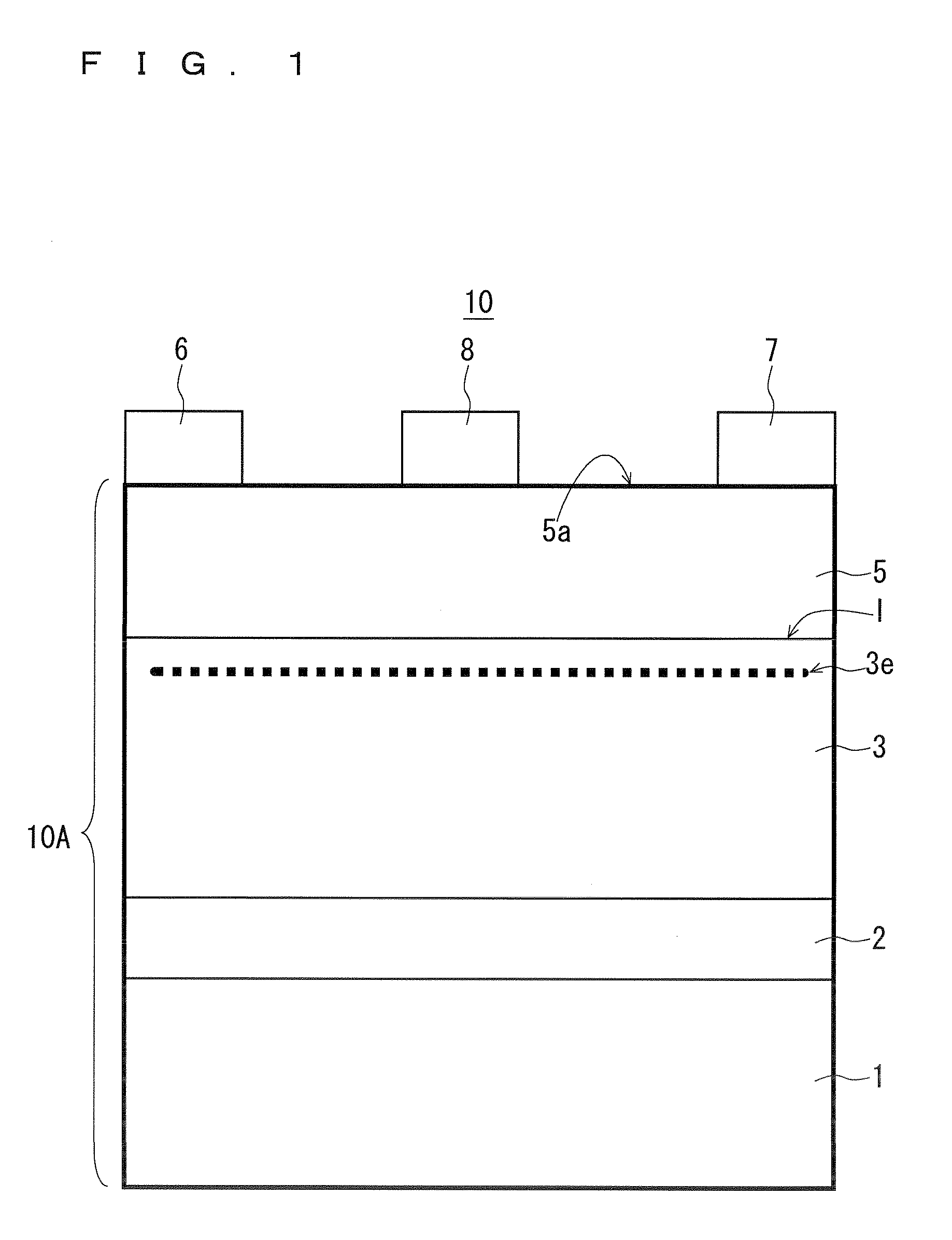
[0031]FIG. 1 is a schematic cross-sectional view schematically showing an epitaxial substrate 10A according to a first embodiment of the present invention and the configuration of a HEMT device 10 manufactured using the same. The epitaxial substrate 10A has the configuration in which a substrate 1, a buffer layer 2, a channel layer 3 and a barrier layer 5 are formed by lamination. As a preferred example, the buffer layer 2, the channel layer 3 and the barrier layer 5 are each epitaxially formed (details thereof are described below) using the metal organic chemical vapor deposition method (MOCVD method). Note that the ratios of the respective layers in FIG. 1 do not reflect actual ones.
[0032]Hereinbelow, description is given of a case where the MOCVD method is used for the formation of each layer. However, other epitaxial growth technique, for example, the method appropriately selected from various vapor phase growth methods and liquid phase growth methods such as MBE, HVPE and...
second embodiment
[0071]
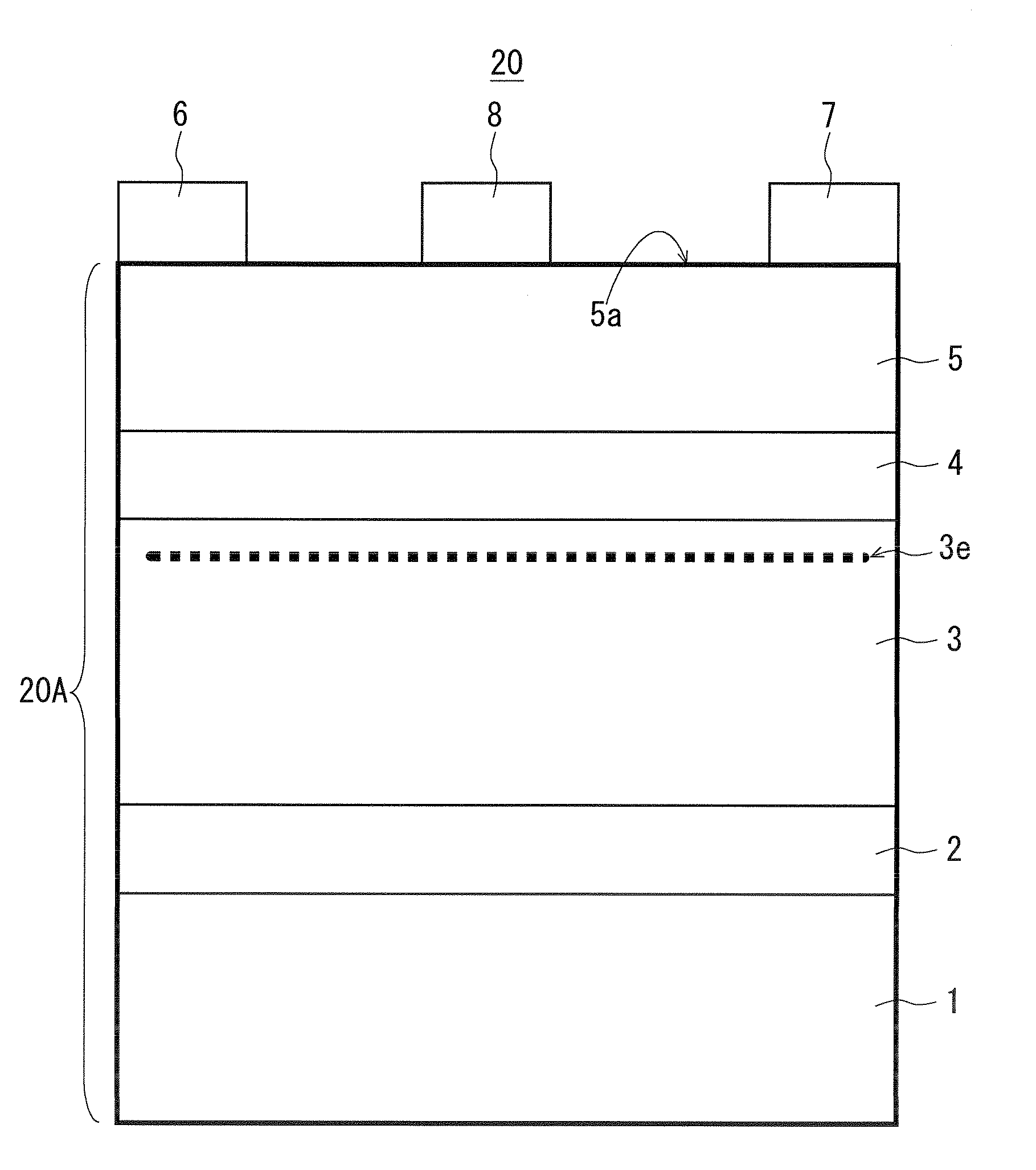
[0072]FIG. 7 is a schematic cross-sectional diagram schematically showing an epitaxial substrate 20A according to a second embodiment of the present invention and the configuration of a HEMT device 20 manufactured using the same. The epitaxial substrate 20A has the configuration in which a spacer layer 4 is interposed between the channel layer 3 and the barrier layer 5 of the epitaxial substrate 10A according to the first embodiment. Constituent elements other than the spacer layer 4 are the same as those of the epitaxial substrate 10A according to the first embodiment, and thus detailed description thereof is omitted.
[0073]The spacer layer 4 is a layer formed of a group III nitride (third group III nitride) that has a composition of Inx3Aly3Gaz3N (x3+y3+z3=1), contains at least Al, and has a bandgap equal to or larger than the bandgap of the barrier layer 5 so as to have a thickness in a range of 1.2 nm±0.2 nm. It has been confirmed that the characteristics of the epitaxial s...
example
[0085]A number of epitaxial substrates 20A were manufactured by variously changing the composition of the barrier layer 5 and the pressure in the reactor in the formation of the barrier layer 5, and characteristics thereof were evaluated. FIG. 8 is a diagram showing a list of the formation conditions for the barrier layer 5 in that case and evaluation results.
[0086]Specifically, the composition of the barrier layer 5 is varied in twelve levels shown in FIG. 8 within the second composition range while the composition of the channel layer 3 is fixed to GaN, and the pressure in the reactor is also varied in four levels shown in FIG. 8 depending on composition, thereby manufacturing 48 types of epitaxial substrates 20A in total.
[0087]Until the formation of the channel layer 3 and the spacer layer 4, a similar procedure was performed in any of the epitaxial substrates 20A.
[0088]First, a 6H-SiC substrate having (0001) plane orientation, having an n-type conductivity and having a diameter ...
PUM
| Property | Measurement | Unit |
|---|---|---|
| thickness | aaaaa | aaaaa |
| thickness | aaaaa | aaaaa |
| mean square roughness | aaaaa | aaaaa |
Abstract
Description
Claims
Application Information