Tunnel field-effect transistor

a field-effect transistor and tunnel-type technology, applied in the direction of instruments, computation using denominational number representation, pulse technique, etc., can solve the problem of limited device-scaling in the sub-65 nm regim

Active Publication Date: 2013-01-24
GLOBALFOUNDRIES US INC
View PDF3 Cites 20 Cited by
  • Summary
  • Abstract
  • Description
  • Claims
  • Application Information

AI Technical Summary

Benefits of technology

[0015]According to another aspect, the present invention provides a method for fabricating a tunnel field-effect transistor, including: providing at least a source region including a corresponding source semiconductor material; providing at least a drain region including a corresponding drain semiconductor material, and providing at least a channel region including a corresponding channel semiconductor material, which is arranged between the source region and the drain region, the method further including: providing at least a source-channel gate electrode on at least an interface between the source region and the channel region; providing at least an insulator corresponding to the source-channel gate electrode between the source-channel gate electrode and at least the interface between the source region and the channel region; providing at least a drain-channel gate electrode on at least an interface between the drain region and the channel region; and providing at least an insulator corresponding to the drain-channel gate electrode between the drain-channel gate electrode and at least the interface between the drain region and the channel region.
[0013]The development of previously-proposed TFETs has been done in order to: improve device performance by, for example, suppressing some of the inherent characteristics of TFETs that are different from those associated with CMOS-based devices, such as, the ambipolar nature of TFETs; improve device switching speeds; and further reduce power dissipation / consumption. Development of TFETs so that they may potentially be applied in diverse logic applications by, for example, harnessing those properties that set it apart from CMOS-based devices has as yet to be addressed.

Problems solved by technology

A drawback associated with CMOS-based devices in, for example, logic applications is that device-scaling in the sub-65 nm regime is limited, not by the intrinsic switching speeds of such devices, but rather by the magnitude of the power that they dissipate.
This may be undesirable, particularly in logic applications, where it is preferable that the “ON” and “OFF” states of a device are distinct.
This structural asymmetry of the TFET may pose some problems for its implementation in certain types of logic applications, such as, for example, pass-gate logic used in SRAM (static random access memory).

Method used


Image

  • Tunnel field-effect transistor
  • Tunnel field-effect transistor
  • Tunnel field-effect transistor

Examples


Embodiment Construction

[0024]Within the description, the same reference numerals or signs have been used to denote the same parts or the like.

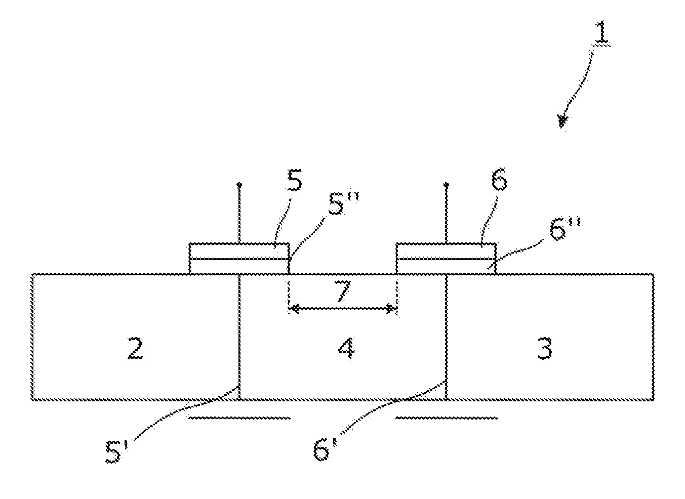
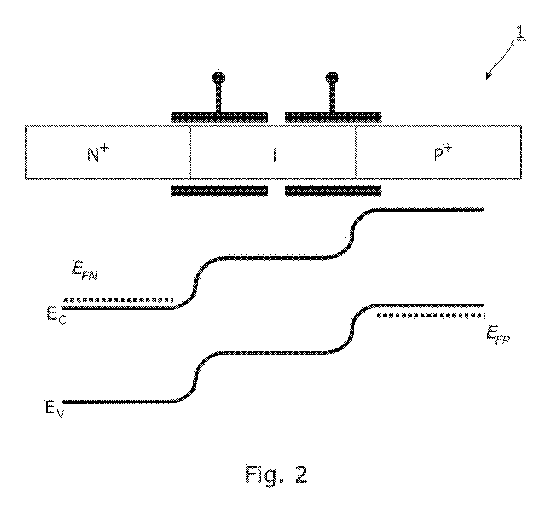
[0025]Reference is now made to FIG. 1, which schematically illustrates an embodiment according to a device aspect of the present invention.

[0026]As can be seen from FIG. 1, an embodiment of the present invention includes a TFET 1 that includes: a source region 2 including a corresponding source semiconductor material; a drain region 3 including a corresponding drain semiconductor material, and a channel region 4 including a corresponding channel semiconductor material, which is provided between the source region 2 and the drain region 3. The source semiconductor material and the drain semiconductor material are doped with carriers such that the polarity of the carriers of the source semiconductor material is different from that of the carriers with which the drain semiconductor material is doped. So, if the source semiconductor material is n-type doped, then the dra...


PUM


Abstract

A tunnel field-effect transistor including at least: a source region including a corresponding source semiconductor material; a drain region including a corresponding drain semiconductor material, and a channel region including a corresponding channel semiconductor material, which is arranged between the source region and the drain region. The tunnel field-effect transistor further includes at least: a source-channel gate electrode provided on an interface between the source region and the channel region; an insulator corresponding to the source-channel gate electrode that is provided between the source-channel gate electrode and the interface between the source region and the channel region; a drain-channel gate electrode provided on an interface between the drain region and the channel region; and an insulator corresponding to the drain-channel gate electrode that is provided between the drain-channel gate electrode and the interface between the drain region and the channel region.

Description

CROSS REFERENCE TO RELATED APPLICATION[0001]This application claims priority under 35 U.S.C. 119 from European Application 11175123.6, filed Jul. 22, 2011, the entire contents of which are incorporated herein by reference.BACKGROUND OF THE INVENTION[0002]1. Field of the Invention[0003]The present invention relates to a tunnel field-effect transistor (TFET) and a method of fabrication therefor.[0004]2. Background of the Invention[0005]Complementary metal-oxide semiconductor (CMOS) technology is used in high-speed switching and logic applications. A drawback associated with CMOS-based devices in, for example, logic applications is that device-scaling in the sub-65 nm regime is limited, not by the intrinsic switching speeds of such devices, but rather by the magnitude of the power that they dissipate. The semiconductor industry has been engaged in seeking a successor to CMOS that has relatively lower power dissipation compared to CMOS and that may be used in logic applications. For dev...

Claims


Application Information

Patent Timeline
Patent Type & Authority Applications(United States)
IPC IPC(8): H01L29/78H03K19/21H01L21/336
CPCH01L29/7391H01L29/42312
Inventor BJOERK, MIKAEL T.DOERING, ANDREAS CHRISTIANSTANLEY-MARBELL, PHILLIPMOSELUND, KIRSTEN EMILIE
Owner GLOBALFOUNDRIES US INC
Why Eureka
Try Eureka