Pattern evaluation method, device therefor, and electron beam device

a technology of electron beam and pattern, applied in the direction of image enhancement, instruments, machines/engines, etc., can solve the problems of lowering throughput, affecting the measurement accuracy of the amount of focus position displacement, and all the reasons for charging cannot be explained, so as to improve the accuracy of focus adjustment or astigmatism correction, improve the speed of measuring the dimension of the pattern with good measurement reproducibility, and improve the effect of resolution

Inactive Publication Date: 2013-01-31
HITACHI HIGH-TECH CORP
View PDF1 Cites 22 Cited by
  • Summary
  • Abstract
  • Description
  • Claims
  • Application Information

AI Technical Summary

Benefits of technology

[0048]According to the present invention with the above configuration, by improving the measurement accuracy of the amount of the focus position displacement or the amount of astigmatic difference by the parallax method, it is possible to improve the accuracy of the focus adjustment or the astigmatism correction. As a result, the speed of measuring the dimension of the pattern with good measurement reproducibility may be improved as compared with a method that uses a contrast in the related art.
[0049]Further, it is possible to provide an electron beam device that is capable of judging irregularities of the periodic pattern formed on a substrate in a short time. Further, it is possible to provide an electron beam device that is capable of judging irregularities under a predetermined optical condition including an accelerating voltage, excitation of the objective lens, and position displacement when the amount of deflection of primary electron beam is changed.

Problems solved by technology

However, as the energy of the electron beam becomes lower, the resolution becomes deteriorated.
However, all reasons of charging cannot be explained.
Therefore, it is required to adjust the focus position displacement or to correct the astigmatic difference, which results in lowering the throughput.
Further, if the charging has in-plane distribution and the charging amount is varied between the chips on the sample, whenever the measuring chip is changed, the focusing adjustment or astigmatism correction described above is required, which results in lowering the throughput.

Method used


Image

  • Pattern evaluation method, device therefor, and electron beam device
  • Pattern evaluation method, device therefor, and electron beam device
  • Pattern evaluation method, device therefor, and electron beam device

Examples


first embodiment

[0091]In a first embodiment, in case of correcting an astigmatism and adjusting a focus from the image acquired in two or more different directions, the amount of correction of a pattern position displacement error depending on the amount of beam deflection and a tilting direction is reflected into a value of an acquired parallax to calculate the astigmatic difference and the amount of focus deviation, thereby correcting the astigmatism and adjusting the focus with high accuracy at a high speed.

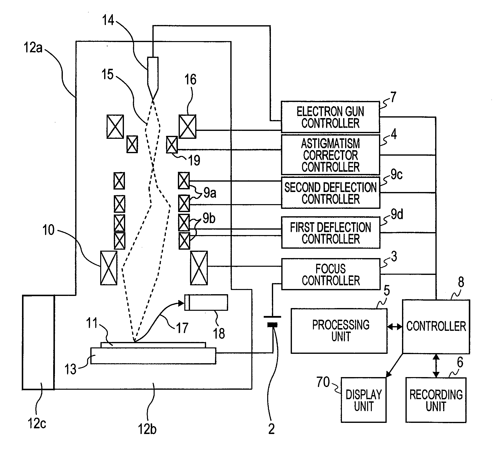
[0092]FIG. 1 is a schematic configuration diagram relating to a casing of a minute pattern evaluation device for measuring a pattern dimension that uses a charged particle beam according to a first embodiment. A wafer 11, which is a sample, is conveyed into a predetermined position in a vacuum sample chamber 12b directly below a casing 12a. In order to observe the wafer 11 that is provided on a wafer holder 13 that functions as a stage in the vacuum sample chamber 12b, a primary electron beam...

second embodiment

[0122]In a second embodiment, in case of correcting an astigmatism and adjusting a focus from the image acquired in two or more different directions, the amount of correction of a pattern position displacement error depending on the amount of beam deflection and a tilting direction is reflected into a beam tilting condition which is a charged particle optical system condition. Accordingly, without correcting in calculating the astigmatic difference and the amount of focus deviation, it is possible to correct the astigmatism and adjust the focus at a high speed with high accuracy. The schematic configuration of a casing of the measuring device that uses a charged particle beam according to the second embodiment is the same as that of FIG. 1.

[0123]FIGS. 10 and 11 show flowcharts of a recipe for automatic measurement according to the second embodiment. In the flowchart of the recipe, the steps before tilting a beam (100 to 108) are the same as those of the first embodiment (40 to 48). ...

third embodiment

[0128]In a third embodiment, in case of adjusting a focus from the image acquired in two or more different directions, the amount of correction of a pattern position displacement error depending on the amount of beam deflection and a tilting direction is reflected into an acquired parallax value to calculate the amount of focus deviation. Since there is no tilting of beam in the plural directions, the focus may be adjusted at a high speed with high accuracy. The schematic configuration of a casing of the measuring device that uses a charged particle beam according to the third embodiment is the same as that of FIG. 1. In the present embodiment, only focus correction is performed without performing the astigmatism correction. The present embodiment is effective for a conductive sample (for example, silicon and the like) in which the astigmatic difference hardly occurs. Since in case of the focus position displacement without astigmatism displacement, the in-focus plane is changed onl...


PUM


Abstract

An amount of pattern position displacement between observation images acquired by irradiating from two different directions is changed depending on beam deflection for moving an image acquisition position. In a pattern evaluation method that measures astigmatic difference or focus position displacement having a small amount of dose at a high speed using parallax caused by the tilted beam, a correction value obtained in advance by measurement is reflected in an amount of pattern position displacement between observation images obtained by irradiating from at least two different directions and generated in accordance with the amount of beam deflection for moving an image acquisition position. A processing unit calculates an amount of correction of an amount of pattern position displacement depending on beam deflection of a beam deflecting unit for moving an image acquisition position on the sample at a high speed.

Description

TECHNICAL FIELD[0001]The present invention relates to a pattern evaluation technology using a charged particle beam that can acquire a two dimensional scanning image indicating a shape or a dimension of a minute pattern formed on a surface of a sample by scanning a charged particle beam onto a surface of the sample (for example, a semiconductor wafer or a reticle) and detecting a secondary charged particle or a reflection particle generated from the sample charged particle microscope, and easily judge irregularities on the surface of the sample.BACKGROUND ART[0002]Currently, a critical dimension scanning electron microscope (hereinafter, abbreviated as CDSEM) is mainly used to measure a dimension of a semiconductor device pattern. The structure of the CDSEM is basically the same as a scanning electron microscope. First of all, an electron discharged from a thermal or field emission electron source is accelerated. Thereafter, an electron beam obtained by reducing a diameter of the el...

Claims


Application Information

Patent Timeline
Patent Type & Authority Applications(United States)
IPC IPC(8): H01J37/26H01J37/20
CPCH01J37/1478H01J37/28H01J2237/24578H01J2237/2611G06T2207/30204G06T7/0044G06T2207/10061G06T2207/30148H01J2237/2817G06T7/74
Inventor YAMANASHI, HIROMASASOHDA, YASUNARIOHASHI, TAKEYOSHIFUKUDA, MUNEYUKI
Owner HITACHI HIGH-TECH CORP
Why Eureka
Try Eureka