Method of forming transparent electrode and fabricating array substrate for liquid crystal display device

Active Publication Date: 2013-01-31
LG DISPLAY CO LTD
View PDF1 Cites 11 Cited by
  • Summary
  • Abstract
  • Description
  • Claims
  • Application Information

AI Technical Summary

Benefits of technology

[0015]Another object of the present invention is to provide a method of fab

Problems solved by technology

Unfortunately, since the LCD device uses the vertical electric field, the device has a bad viewing angle.
On the other hand, some problems are caused in the photolithography process for a transparent conductive material.
Namely, a width of the pixel electrode obtained by the photolithography pr

Method used


Image

  • Method of forming transparent electrode and fabricating array substrate for liquid crystal display device
  • Method of forming transparent electrode and fabricating array substrate for liquid crystal display device
  • Method of forming transparent electrode and fabricating array substrate for liquid crystal display device

Examples


Embodiment Construction

[0025]Reference will now be made in detail to the preferred embodiments, examples of which are illustrated in the accompanying drawings.

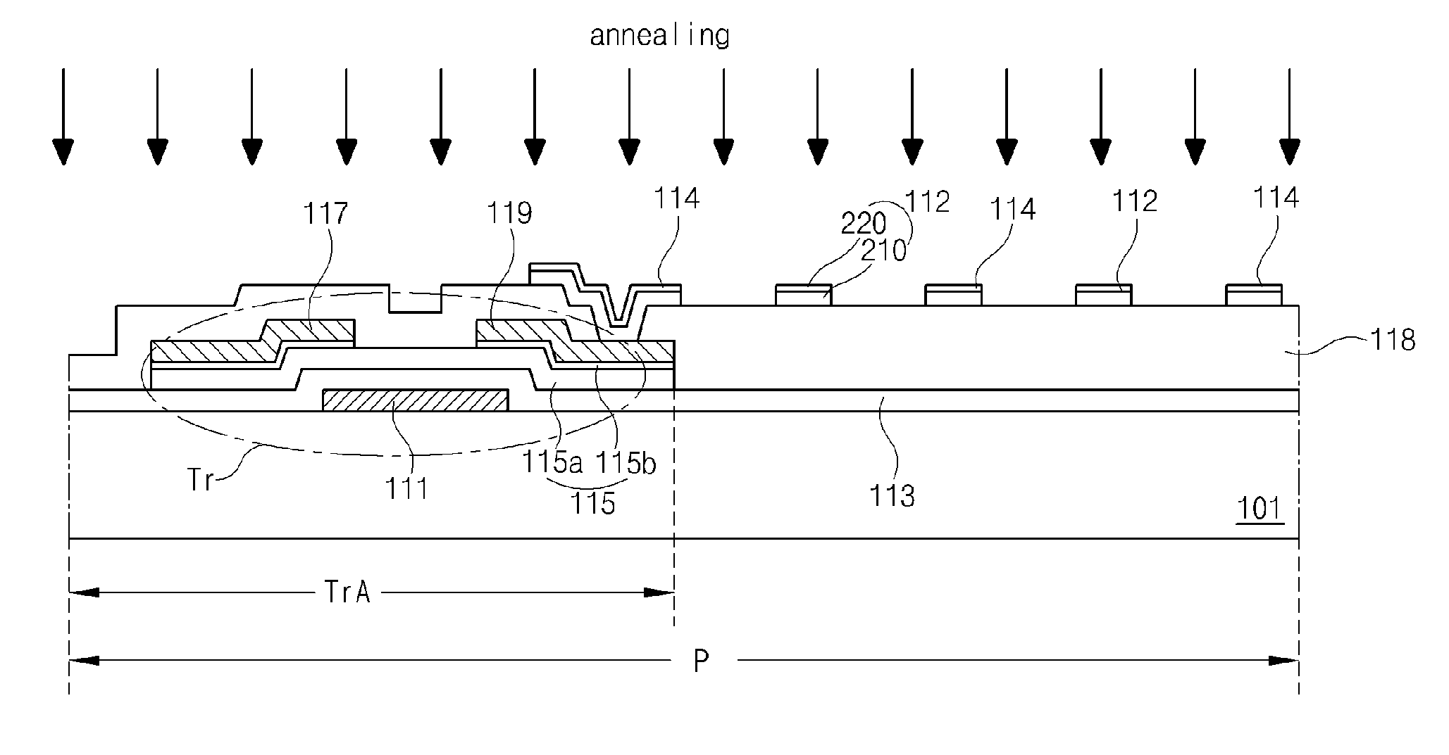
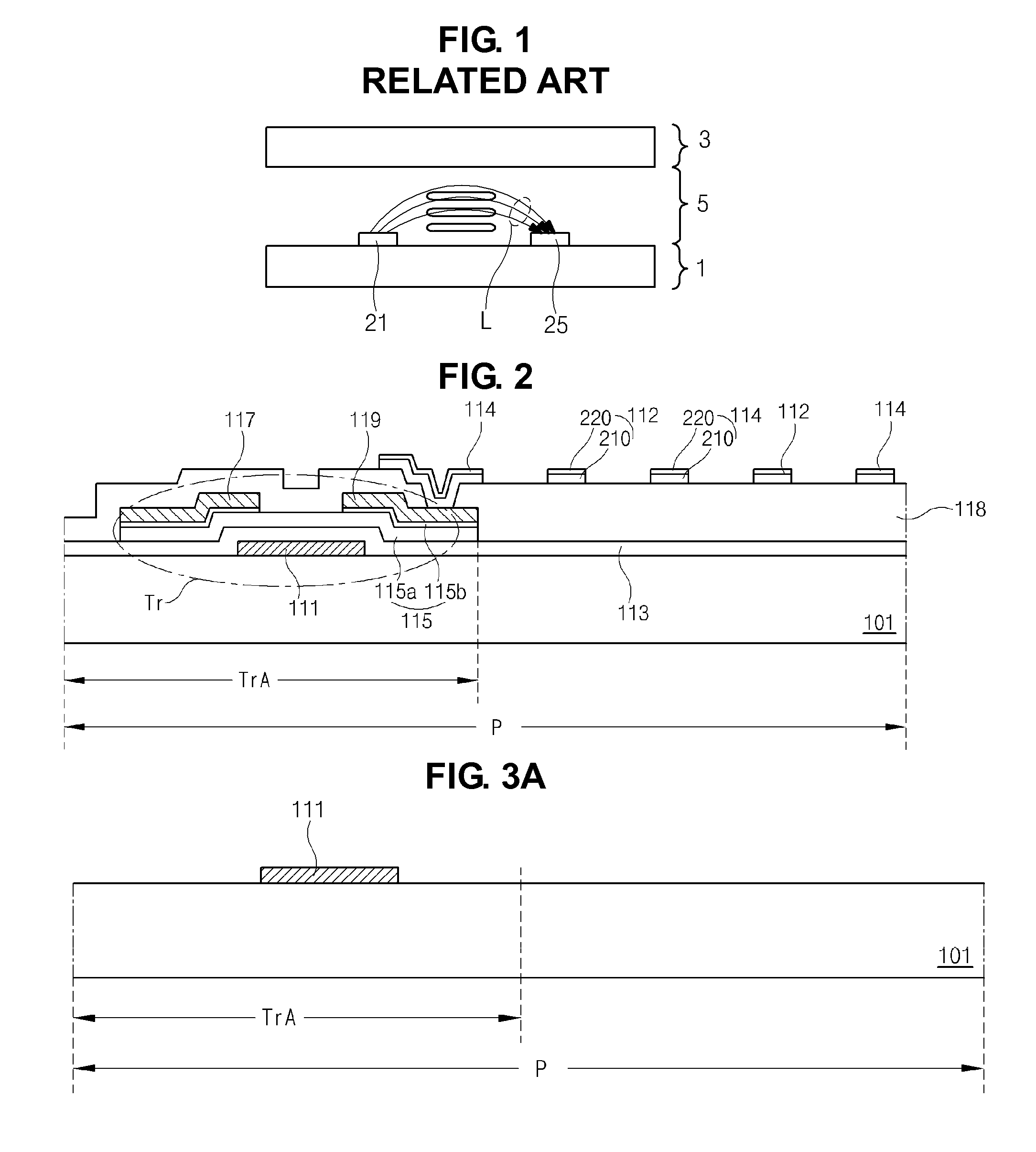
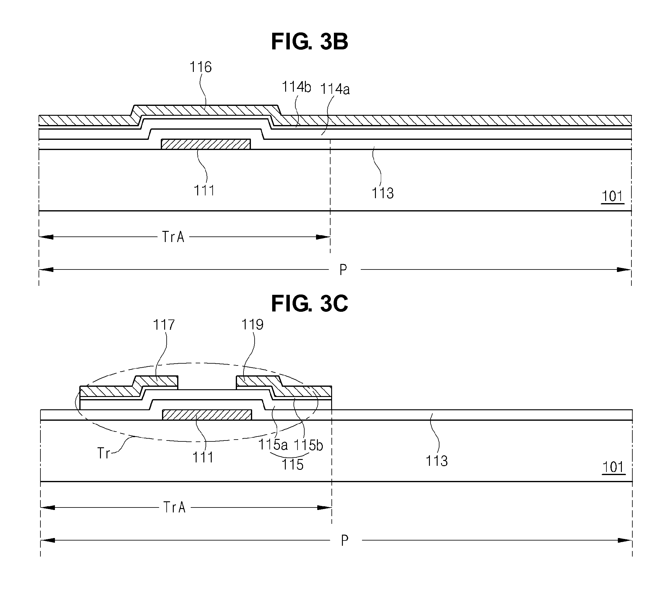
[0026]FIG. 2 is a cross-sectional view of an array substrate for an LCD device according to the present invention. A patterning method and a fabricating method of the present invention can be used for any device including a transparent conductive material pattern such as a pixel electrode and a common electrode. Hereinafter, the patterning method and the fabricating method of the present invention are explained with the array substrate for the IPS mode LCD device.

[0027]Referring to FIG. 2, an array substrate for an IPS mode LCD device includes a substrate 101, a gate line (not shown), a data line (not shown), a common line (not shown), a thin film transistor (TFT) Tr, a common electrode 112 and a pixel electrode 114.

[0028]The common line is parallel to and spaced apart from the gate line. The data line crosses the gate line to define a pixel region ...


PUM


Abstract

A method of forming a transparent electrode includes forming a first transparent conductive material layer on a base; performing a plasma process on the first transparent conductive material layer such that the upper portion of the first transparent conductive material layer is changed into semitransparent; forming a second transparent conductive material layer on the first transparent conductive material layer; patterning the second transparent conductive material layer and the first transparent conductive material layer; and annealing the patterned second transparent conductive material layer and the patterned first transparent conductive material layer such that the upper portion of the first transparent conductive material layer is changed into transparent.

Description

[0001]The present application claims the benefit of Korean Patent Application No. 10-2011-0074423 filed in Korea on Jul. 27, 2011, which is hereby incorporated by reference.BACKGROUND OF THE INVENTION[0002]1. Field of the Invention[0003]The present invention relates to a liquid crystal display (LCD) device and more particularly to a method of forming transparent electrode and fabricating an array substrate for an LCD device being capable of preventing a problem in a patterning process resulted from reflection of light by a chuck.[0004]2. Discussion of the Related Art[0005]The LCD device, which uses an optical anisotropy and a polarization property to display an image, is widely used for notebook computers, monitors, TV, and so on, because of their high contrast ratio and characteristics adequate to display moving images.[0006]The LCD device includes a liquid crystal panel having a first substrate, a second substrate and a liquid crystal layer. The first and second substrates face ea...

Claims


Application Information

Patent Timeline
IPC IPC(8): H01L33/42B44C1/22B05D5/12
CPCH01L27/124G02F1/1343
Inventor KIM, YONG-ILKIM, JEONG-OHHONG, GI-SANGBEAK, JUNG-SUN
Owner LG DISPLAY CO LTD
Why Eureka
Try Eureka