MEMS resonator and electrical device using the same
a technology of mems resonator and electrical device, which is applied in the direction of oscillator, electrical apparatus, multiple-port network, etc., to achieve the effect of increasing the size and cost of a mems resonator and reducing the frequency of resonan
- Summary
- Abstract
- Description
- Claims
- Application Information
AI Technical Summary
Benefits of technology
Problems solved by technology
Method used
Image

Examples
first embodiment
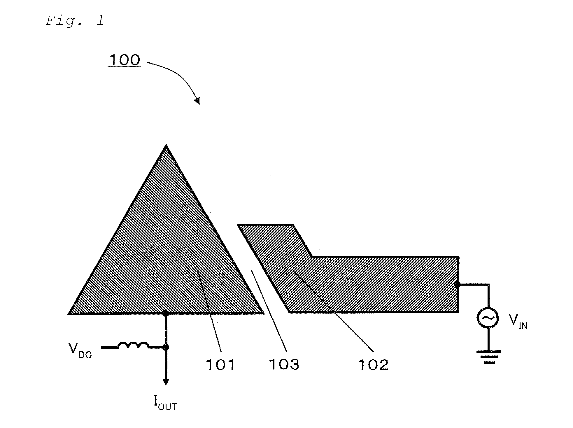
[0064]FIG. 1 is a cross sectional view showing a structure of an oscillator and an electrode of a MEMS resonator of the present embodiment. A MEMS resonator 100 shown in FIG. 1 includes a flexible oscillator 101 and an electrode 102. FIG. 1 show a cross section along a plane perpendicular to the longitudinal direction of the oscillator 101, and the oscillator 101 is of a triangular cross-section beam structure. The oscillator 101 oscillates in a torsional oscillation mode with the center being its longitudinal axis (the direction perpendicular to the plane of the drawing). In FIG. 1, the oscillator 101 and the electrode 102 are opposed to each other at a sloped face of the oscillator 101, so as to form an electrostatic capacitance.
[0065]In the embodiment shown in the drawing, the oscillator 101 is an output electrode (i.e. detection electrode) and the electrode 102 is an input electrode (i.e. excitation electrode). A signal generated by the oscillator 101 is output from a supporter ...
second embodiment
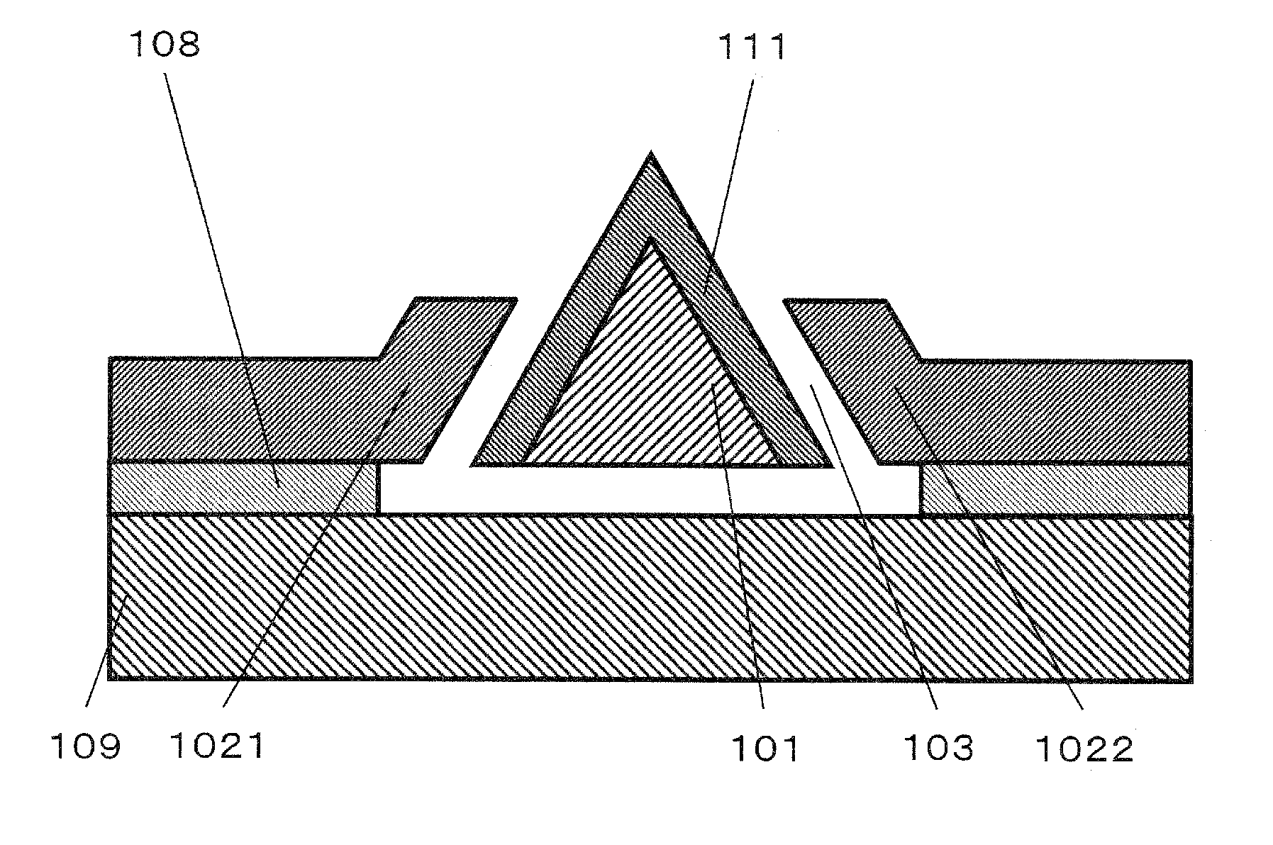
[0081]FIG. 5 is a cross sectional view showing a structure of an oscillator and an electrode of a MEMS resonator of a second embodiment. A MEMS resonator 200 shown in FIG. 5 includes an oscillator 101 that is of a triangular cross-section beam structure and an electrode 102, similarly to the MEMS resonator 100 of the first embodiment. In the present embodiment, the oscillator 101 is an output electrode, and the electrode 102 is an input electrode. A signal generated in the oscillator 101 is output from a supporter (not shown) that oscillatably supports the oscillator 101. In FIG. 5, the oscillator 101 and electrode 102 are opposing to each other at a sloped face of the oscillator 101, so as to form an electrostatic capacitance.
[0082]The MEMS resonator 200 shown in FIG. 5 is different from the MEMS resonator 100 of the first embodiment in that a high-doped area 111 is formed in the surface part of the oscillator 101 including the opposing face to the electrode 102, where an impurity ...
third embodiment
[0091]FIG. 6 is a cross sectional view showing a structure of an oscillator and electrode of a MEMS resonator of a third embodiment.
[0092]A MEMS resonator 300 shown in FIG. 6 includes a movable oscillator 101, an input electrode 1021 and an output electrode 1022. In the MEMS resonator 300 shown in FIG. 6, the oscillator 101 is opposed to each of the input electrode 1021 and output electrode 1022 at two respective sloped faces of the oscillator 101. A DC power source is connected to the oscillator 101 through a supporter (not shown) that oscillatably supports it, so as to supply a DC voltage between the oscillator 101 and the electrode 1021 and between the oscillator 101 and the electrode 1022. The oscillator 101 is excited by an AC voltage applied to the electrode 1021, and a high frequency signal of the resonance frequency is output from the electrode 1022.
[0093]In the microelectromechanical resonator 300 shown in FIG. 6, the oscillator 101 and the input and output electrodes 1021 ...
PUM
 Abstract
Description
Claims
Application Information
 - R&D
- Intellectual Property
- Life Sciences
- Materials
- Tech Scout
- Unparalleled Data Quality
- Higher Quality Content
- 60% Fewer Hallucinations
Browse by: Latest US Patents, China's latest patents, Technical Efficacy Thesaurus, Application Domain, Technology Topic, Popular Technical Reports.
© 2025 PatSnap. All rights reserved.Legal|Privacy policy|Modern Slavery Act Transparency Statement|Sitemap|About US| Contact US: help@patsnap.com