Electrode foil and organic device

a technology of electrodes and foils, applied in the field of electrodes, can solve the problems of low heat resistance and barrier performance, low thermal conductivity, and low material cost, and achieve the effect of superior thermal conductivity

Inactive Publication Date: 2013-02-28
MITSUI MINING & SMELTING CO LTD
View PDF4 Cites 9 Cited by
  • Summary
  • Abstract
  • Description
  • Claims
  • Application Information

AI Technical Summary

Benefits of technology

[0014]The inventors have currently found that extremely smoothing at least one surface of a metal foil enables attainment of an electrode foil useful for flexible electronic devices, which has all the functions of a supporting base material, an electrode and a reflective layer and also has a superior thermal conductivity.

Problems solved by technology

The ultra-thin glass is superior in heat resistance, barrier performance and optical transparency and has good flexibility, but is somewhat inferior in handling and has low thermal conductivity and high material cost.
Further, the resin film is superior in handling and flexibility and has low material cost and good optical transparency, but is inferior in heat resistance and barrier performance and has low thermal conductivity.

Method used


Image

  • Electrode foil and organic device
  • Electrode foil and organic device
  • Electrode foil and organic device

Examples


example 1

Preparation of Cu / Al-Alloy / ITO Electrode Foil

[0068]As a metal foil, 64-μm-thick commercially available both-side-flat electrolytic copper foil (DFF (Dual Flat Foil), manufactured by Mitsui Mining & Smelting Co., Ltd.) was prepared. The surface roughness of the copper foil was measured with a scanning probe microscope (Nano Scope V, manufactured by Veeco Instrument Inc.) in accordance with JIS B0601-2001, resulting in an arithmetic average roughness Ra of 12.20 nm. This measurement was performed in an area of 10 μm square using a Tapping Mode AFM.

[0069]The copper foil was subjected to CMP (Chemical Mechanical Polishing) treatment with a polishing machine manufactured by MAT Inc. This CMP treatment was performed by using a polishing pad having XY grooves and a colloidal silica polishing liquid under the conditions of pad rotation speed of 30 rpm; load of 200 gf / cm2; and liquid supply rate of 100 cc / min. The copper foil thus treated with CMP was subjected to measurement of the surface ...

example 2

Preparation of Cu / Al-Alloy / C Electrode Foil

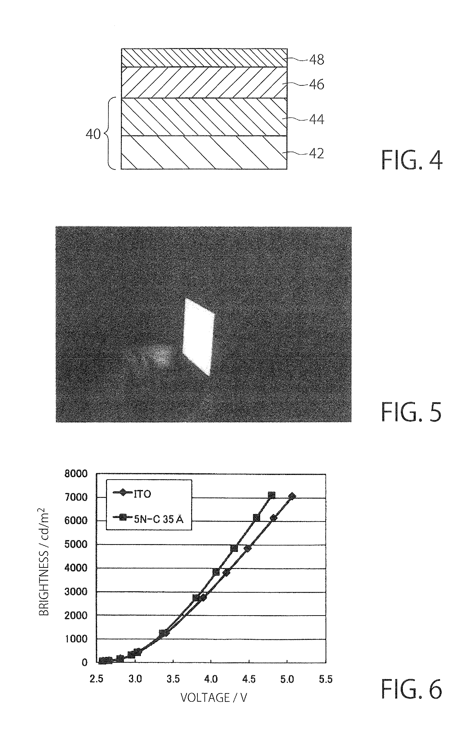
[0072]An electrode foil was prepared in the same manner as in Example 1 except that a carbon buffer layer with a thickness of 1.7 nm or 3.5 nm was formed by sputtering in place of the ITO buffer layer. As a carbon target for the sputtering, two types of carbon targets were prepared including a non-treated carbon target with a purity of 3N (99.9%) made from a carbon material (IGS743, manufactured by Tokai Carbon Co., Ltd.); and a carbon target having a purity of 5N (99.999%) made from the above carbon material through purification treatment with a halogen gas. By using each of these targets, the carbon buffer layer was formed by sputtering. This sputtering was performed under the conditions of input power (DC) of 250 W (0.8 W / cm2); ultimate vacuum of lower than 5×10⁻⁵ Pa; sputtering pressure of 0.5 Pa; Ar flow rate of 100 sccm; and substrate temperature at room temperature, after mounting each carbon target (203.2 mm diameter and 8 mm thick)...

example 3

Preparation of Cu / C Electrode Foil

[0073]An electrode foil having a carbon buffer layer was prepared in the same manner as in Example 2 except that the Al alloy reflective layer was not formed. The surface roughness of the buffer layer thus obtained was measured in the same manner as in Example 1, resulting in an arithmetic average roughness Ra of 1.42 nm. The total thickness of the resulting electrode foil was 48 μm.


PUM

PropertyMeasurementUnit
arithmetic average roughnessaaaaaaaaaa
thicknessaaaaaaaaaa

Abstract

There are provided an electrode foil which has all the functions of a supporting base material, an electrode and a reflective layer and also has a superior thermal conductivity; and an organic device using the same. The electrode foil comprises a metal foil, wherein the electrode foil has at least one outermost surface which is an ultra-smooth surface having an arithmetic average roughness Ra of 10.0 nm or less as measured in accordance with JIS B 0601-2001.

Description

CROSS-REFERENCE TO RELATED APPLICATION[0001]This application claims priority to Japanese Patent Application No. 2010-129083 filed on Jun. 4, 2010, the entire disclosure of which is incorporated herein by reference.TECHNICAL FIELD[0002]The present invention relates to an electrode foil using a metal foil, and to an organic device using the electrode foil, such as an organic EL element, an organic EL lighting, an organic solar cell or the like.BACKGROUND ART[0003]In recent years, organic EL lighting has been drawing attention as an eco-friendly green device. Features of the organic EL lighting include: 1) a low power consumption as compared with an incandescent lamp; 2) a thin profile and light weight; and 3) a flexibility. At the moment, the organic EL lightings are being developed so as to attain the above features of 2) and 3). In this respect, glass substrates that have been conventionally used in flat panel displays (FPD) are unable to attain the above features of 2) and 3).[0004...

Claims


Application Information

Patent Timeline
Patent Type & Authority Applications(United States)
IPC IPC(8): H05B33/26B32B15/04B32B33/00H01B1/02H01L51/52H01L51/44
CPCH01L51/441Y10T428/12431H01L2251/5315H01L2251/5353H01L2251/55H05B33/26Y02E10/549C22F1/08C25D5/48C25D7/0614H01L51/0097H01L51/5012H01L51/5203Y10T428/12438Y10T428/12993H01L51/5221Y10T428/31678Y02P70/50H10K77/111H10K30/81H10K50/82H10K2102/3026H10K2102/321H10K2101/00H10K50/805H10K50/11
Inventor MATSUURA, YOSHINORIKITAJIMA, NOZOMUABE, NAOHIKO
Owner MITSUI MINING & SMELTING CO LTD
Why Eureka
Try Eureka