Mosfet including asymmetric source and drain regions

a technology of mosfet and drain region, which is applied in the field of mosfet including asymmetric source and drain region, can solve the problem that the overlap capacitance between the gate electrode and the source extension region of the field effect transistor does not provide a corresponding benefit, and achieves less drain-side overlap capacitance, less source-side external resistance, and greater thickness

Inactive Publication Date: 2013-02-28
IBM CORP
View PDF3 Cites 59 Cited by
  • Summary
  • Abstract
  • Description
  • Claims
  • Application Information

AI Technical Summary

Benefits of technology

[0005]Angled ion implantation that structurally damages a single crystalline surface of a semiconductor surface can retard the epitaxial growth of a semiconductor material thereupon. At least one drain-side surfaces of a field effect transistor (FET) structure, which can be a structure for a planar FET or a fin FET, is structurally damaged by an angled ion implantation of inert or electrically active dopants, while at least one source-side surface of the transistor is protected from implantation by a gate stack and a gate spacer. Epitaxial growth of a semiconductor material is retarded on the at least one structurally damaged drain-side surface, while epitaxial growth proceeds without retardation on the at least one source-side surface. A raised epitaxial source region has a greater ...

Problems solved by technology

However, reducing the overlap capacitance between the gate electrode and a source ...

Method used


Image

  • Mosfet including asymmetric source and drain regions
  • Mosfet including asymmetric source and drain regions
  • Mosfet including asymmetric source and drain regions

Examples


first embodiment

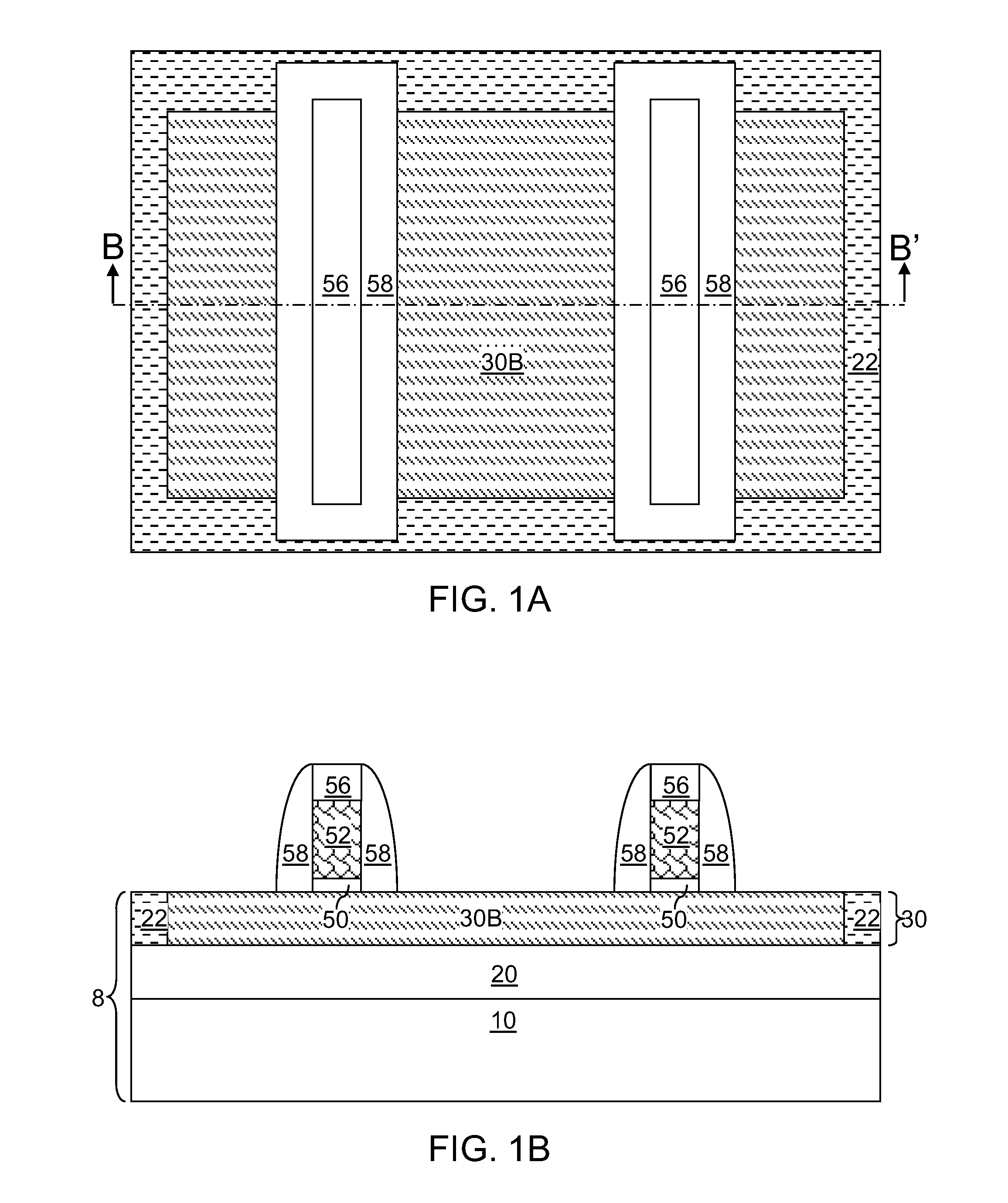
[0023]Referring to FIGS. 1A and 1B, a first exemplary semiconductor structure according to the present invention includes a semiconductor substrate 8 and gate structures formed thereupon. The semiconductor substrate 8 can be a semiconductor-on-insulator (SOI) substrate including a stack, from bottom to top, of a handle substrate 10, a buried insulator layer 20, and a top semiconductor layer 30. Alternately, the semiconductor substrate 8 can be a bulk substrate including a semiconductor material therein.

[0024]The semiconductor substrate 8 includes a semiconductor material region having an exposed top semiconductor surface. If the semiconductor substrate 8 is an SOI substrate, the semiconductor material region can be located in the top semiconductor layer 30. If the semiconductor substrate 8 is a bulk semiconductor substrate (not shown), the semiconductor material portion can be a top portion of the bulk semiconductor substrate. Shallow trench isolation structures 22 including a diele...

third embodiment

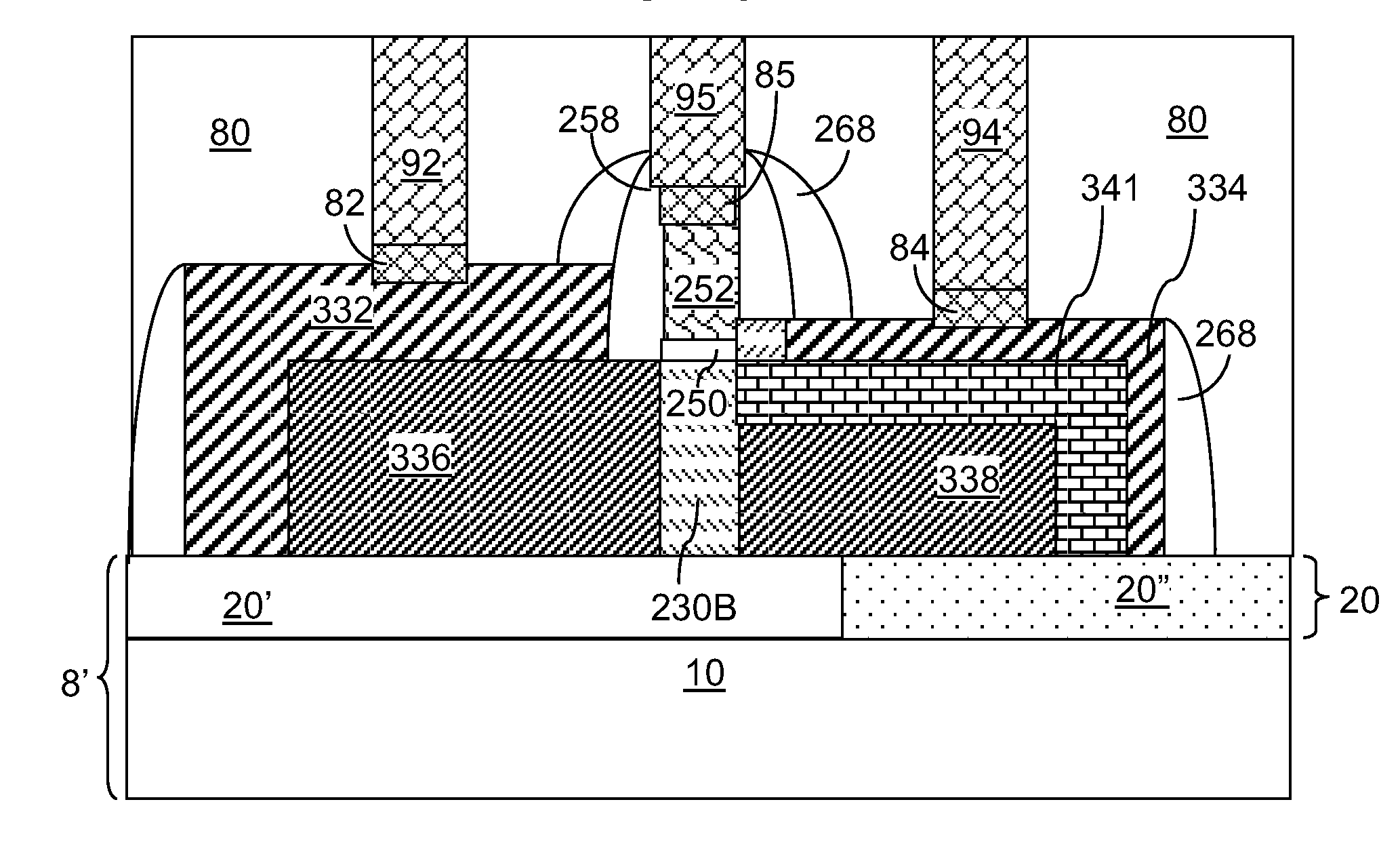
[0090]Referring to FIGS. 11A and 11B, a third exemplary semiconductor structure according to the present disclosure can be derived from the second exemplary semiconductor structure of FIGS. 7A, 7B, and 7C by selectively depositing an intrinsic semiconductor material instead of an in-situ doped semiconductor material. Specifically, selective epitaxy is performed to deposit an intrinsic semiconductor material on the exposed semiconductor surfaces of the structurally damaged regions 239 (See FIGS. 7A, 7B, and 7C) and the semiconductor fin portions 230. Because the structurally damaged regions 239 include surface defects that impede the mobility of adatoms from the reactant, an epitaxial semiconductor material portion deposited on the structurally damaged regions 239 has a lesser thickness than another epitaxial semiconductor material portion deposited directly on the semiconductor fin portions 230.

[0091]Because the selective epitaxy is performed at an elevated temperature that is suffi...


PUM


Abstract

At least one drain-side surfaces of a field effect transistor (FET) structure, which can be a structure for a planar FET or a fin FET, is structurally damaged by an angled ion implantation of inert or electrically active dopants, while at least one source-side surface of the transistor is protected from implantation by a gate stack and a gate spacer. Epitaxial growth of a semiconductor material is retarded on the at least one structurally damaged drain-side surface, while epitaxial growth proceeds without retardation on the at least one source-side surface. A raised epitaxial source region has a greater thickness than a raised epitaxial drain region, thereby providing an asymmetric FET having lesser source-side external resistance than drain-side external resistance, and having lesser drain-side overlap capacitance than source-side overlap capacitance.

Description

BACKGROUND[0001]The present disclosure relates to semiconductor structures, and more particularly to planar and fin field effect transistor (FET) structures having asymmetric source and drain regions, and methods of manufacturing the same.[0002]The source-side external resistance and the drain-side external resistance of a field effect transistor impact the performance of the field effect transistor in different ways. For example, external resistance due to a source region or a source extension region has a significant impact both on the linear-regime drain current (Idlin) and the saturation drain current (Idsat) of a field effect transistor. In contrast, external resistance due to a drain region or a drain extension region has a significant impact on the linear-regime drain current of the field effect transistor, but does not impact the saturation drain current of the field effect transistor.[0003]Further, reducing the overlap capacitance between a gate electrode and a drain extens...

Claims


Application Information

Patent Timeline
IPC IPC(8): H01L29/78H01L21/336
CPCH01L29/66803H01L29/785H01L21/823418H01L21/84H01L21/26586H01L29/66477H01L21/26513H01L29/6656H01L29/66628H01L29/66659H01L29/66045H01L21/26506
Inventor CHENG, KANGGUOHARAN, BALASUBRAMANIAN S.PONOTH, SHOMSTANDAERT, THEODORUS E.YAMASHITA, TENKO
Owner IBM CORP
Why Eureka
Try Eureka