Multi charged particle beam writing apparatus and multi charged particle beam writing method

Active Publication Date: 2013-03-07
NUFLARE TECH INC
View PDF8 Cites 39 Cited by
  • Summary
  • Abstract
  • Description
  • Claims
  • Application Information

AI Technical Summary

Benefits of technology

[0009]In accordance with one aspect of this invention, a multi charged particle beam writing apparatus includes a stage on which a target object is placed and which is continuously movable; an emitting unit configured to emit charged particle beam; an aperture member, in which a plurality of openings are formed, configured to receive irradiation of the charged particle beam on a region including all the plurality of openings, and to form multi-beams by making portions of the charged particle beam pass through the plurality of openings; a plurality of blankers configured to perform blanking-deflect regarding beams corresponding to the multi-beams passing through the plurality of openings of the aperture member, respectively; a blanking aperture member configured to shield each of the beams deflected by the plurality of blankers so that the beams deflected by the plurality of blankers are beam-off; a deflector configured to deflect beams together, which have passed through the blanking aperture member, at each irradiation position of each beam on the target object; a writing processing control unit configured to control writing processing with a plurality of beams having passed through di

Problems solved by technology

As a result, it is difficult to set the lens condition to an optimized state together with a lot of other parameters required for the optical system so that the size precision becomes high precision.
In the case of mechanical rotation fitting, adjustment of an accurate rotational position of an nm order is required, which is not realistic.
As fabrication precision, in order to adjust the fabrication precision to precision of, for example, nm or less (for example, 0.1 nm), a significantly close design is required, which is not also realistic.
In designing the optical system, even though the optical system may be designed with high precision, setting ranges of other design parameters are limited.
As a result, when field deformation intends to be modified, optimization of these other conditions (for example, resolution perfor

Method used


Image

  • Multi charged particle beam writing apparatus and multi charged particle beam writing method
  • Multi charged particle beam writing apparatus and multi charged particle beam writing method
  • Multi charged particle beam writing apparatus and multi charged particle beam writing method

Examples


first embodiment

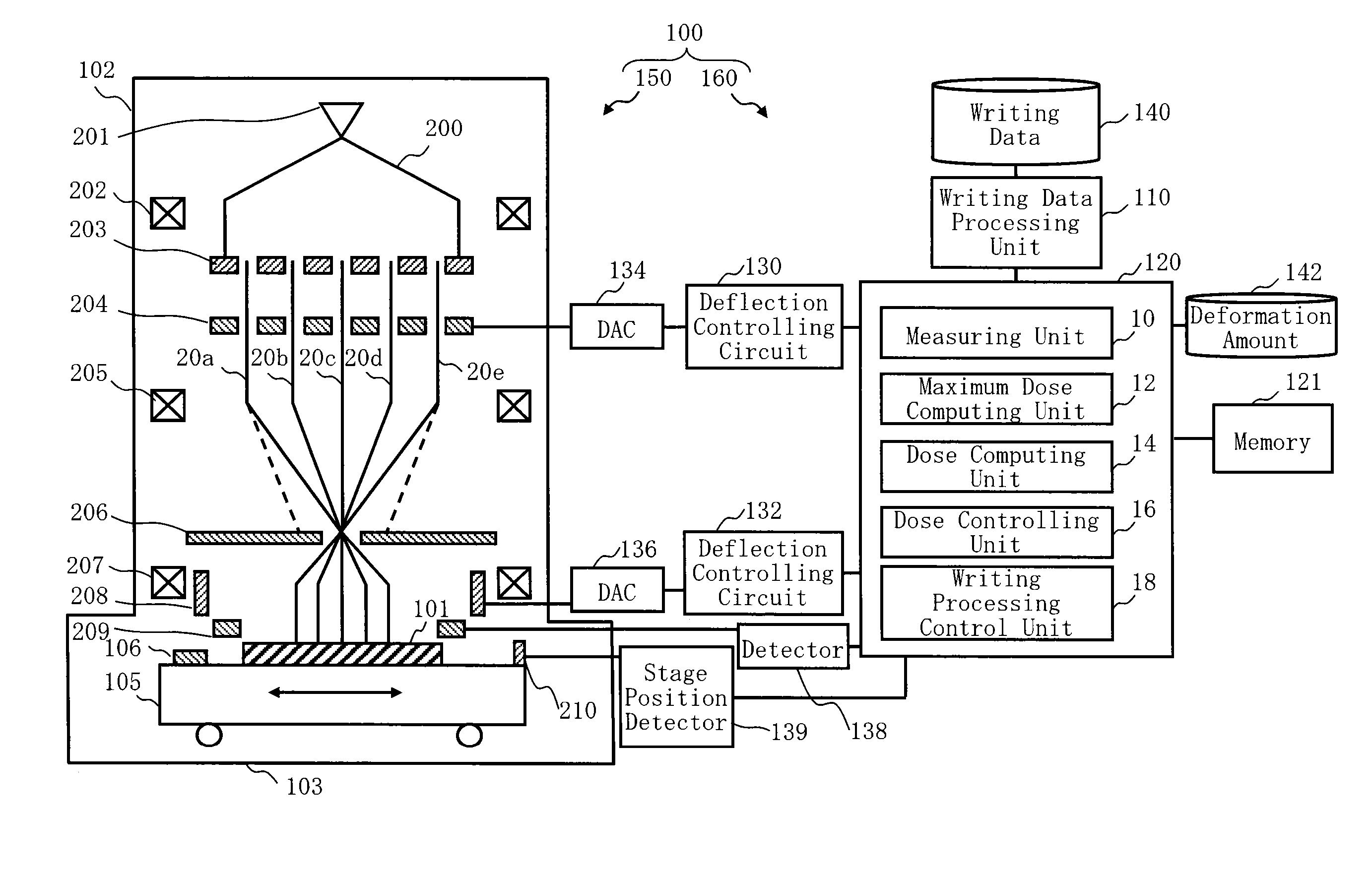
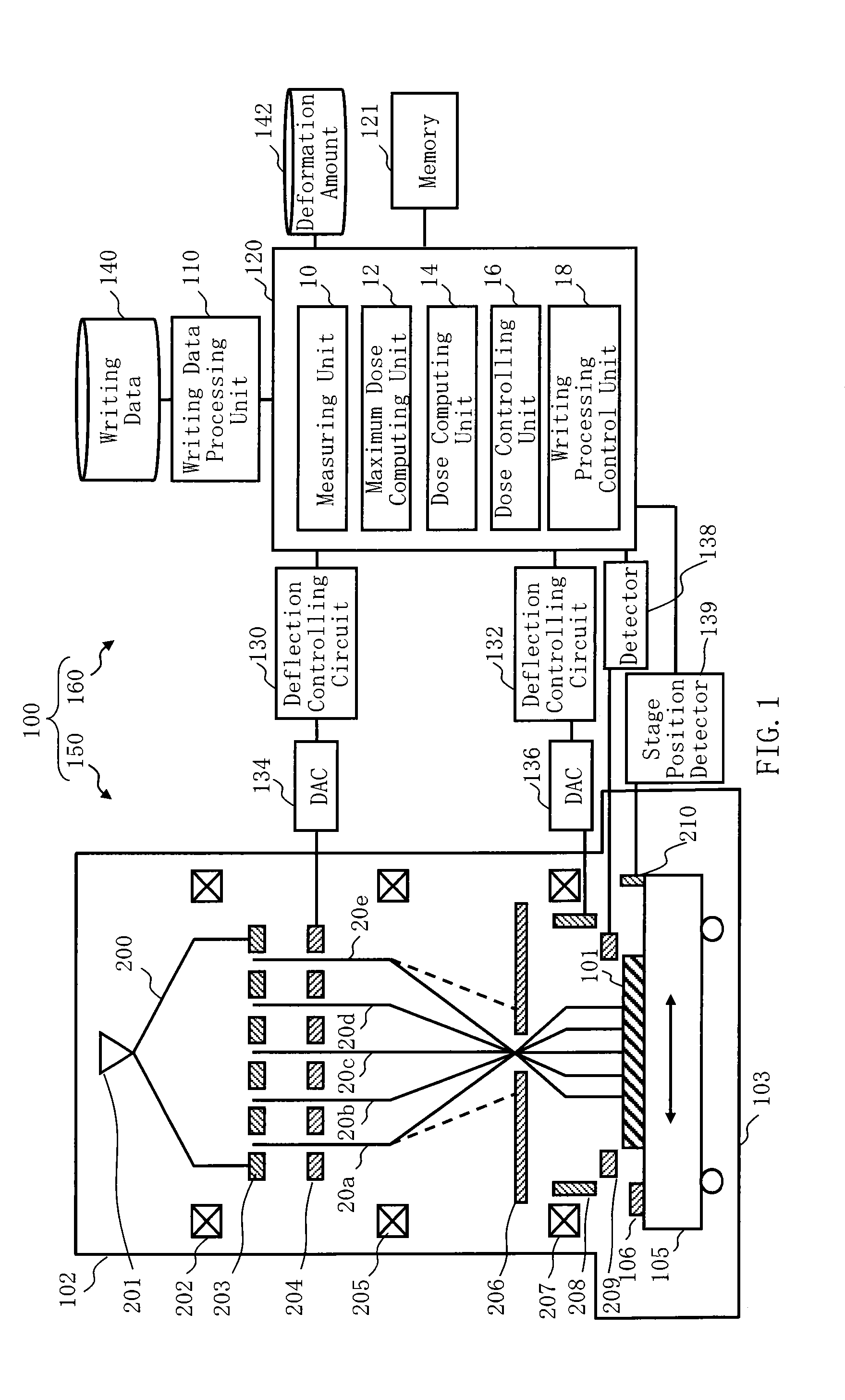
[0028]FIG. 1 is a conceptual diagram illustrating a configuration of a writing apparatus in a first embodiment. In FIG. 1, a writing apparatus 100 (or “drawing apparatus”) includes a writing unit 150 and a control unit 160. The writing apparatus 100 is one example of a multi charged particle beam writing apparatus. The writing unit 150 includes an electron lens barrel 102 and a writing chamber 103. In the electron lens barrel 102, an electron gun 201, an illumination lens 202, an aperture member 203, a blanking plate 204, a reduction lens 205, a limiting aperture member 206, an objective lens 207, a deflector 208, and a detector 209 are placed. In the writing chamber 103, an XY stage 105 is placed. On the XY stage 105, a target object 101 such as a mask serving as a substrate to be written or “drawn” while writing or “drawn” is placed. An exposure mask at the time of fabricating a semiconductor device or a semiconductor substrate (silicon wafer) where the semiconductor device is fab...


PUM


Abstract

In accordance with one aspect of this invention, a multi charged particle beam writing apparatus includes an aperture member, in which a plurality of openings are formed, configured to form multi-beams by making portions of the charged particle beam pass through the plurality of openings; a plurality of blankers configured to perform blanking-deflect regarding beams corresponding to the multi-beams; a writing processing control unit configured to control writing processing with a plurality of beams having passed through different openings among the plurality of openings being irradiated on the target object at a predetermined control grid interval; and a dose controlling unit configured to variably control a dose of a beam associated with deviation according to a deviation amount when an interval between the plurality of beams irradiated is deviated from the control grid interval.

Description

CROSS-REFERENCE TO RELATED APPLICATION[0001]This application is based upon and claims the benefit of priority from prior Japanese Patent Application No. 2011-190957 filed on Sep. 1, 2011 in Japan, the entire contents of which are incorporated herein by reference.BACKGROUND OF THE INVENTION[0002]1. Field of the Invention[0003]Embodiments described herein relate generally to a multi charged particle beam writing apparatus and a multi charged particle beam writing method, and for example, a method for making a plurality of irradiation positions by multi-beams with high precision.[0004]2. Related Art[0005]A lithography technique that is charge in the progress of refinement of a semiconductor device is a very important process to generate a unique pattern in a semiconductor fabricating process. In recent years, with high integration of LSI, a line width of a circuit required for the semiconductor device has been refined every year. Herein, an electron ray (electron beam) writing techniqu...

Claims


Application Information

Patent Timeline
IPC IPC(8): G21K5/04
CPCH01J37/3026H01J37/3177H01J2237/31764H01J2237/31766H01L21/3085B82Y10/00B82Y40/00H01L21/2633H01L21/263H01J37/3174
Inventor YOSHIKAWA, RYOICHIOGASAWARA, MUNEHIRO
Owner NUFLARE TECH INC
Why Eureka
Try Eureka