Defect gradient to boost nonvolatile memory performance

a nonvolatile memory and gradient technology, applied in the direction of bulk negative resistance effect devices, semiconductor devices, electrical equipment, etc., can solve the problems of insufficient resistance of high-to-low resistance films and/or the ratio of high-to-low resistance states to be of use within a practical nonvolatile memory device, and the magnitude of the difference between states and differences between states throughout the life of the device is often not desirabl

Active Publication Date: 2013-03-07
KIOXIA CORP +1
View PDF1 Cites 29 Cited by
  • Summary
  • Abstract
  • Description
  • Claims
  • Application Information

AI Technical Summary

Benefits of technology

[0020]Embodiments of the invention may further provide a resistive nonvolatile memory element that includes a first electrode, a stoichiometric metal oxide layer disposed on the first electrode, a defect layer disposed on the stoichiometric metal oxide layer, the defect layer comprising alternating layers of the stoichiometric metal oxide ...

Problems solved by technology

However, as device dimensions shrink, scaling issues are posing challenges for traditional nonvolatile memory technology.
Although metal oxide (MO) films such as these exhibit bistability, the resistance of these films and/or the ratio of the high-to-low resistance states is (are) often insufficient to be of use within a pr...

Method used


Image

  • Defect gradient to boost nonvolatile memory performance
  • Defect gradient to boost nonvolatile memory performance
  • Defect gradient to boost nonvolatile memory performance

Examples


Embodiment Construction

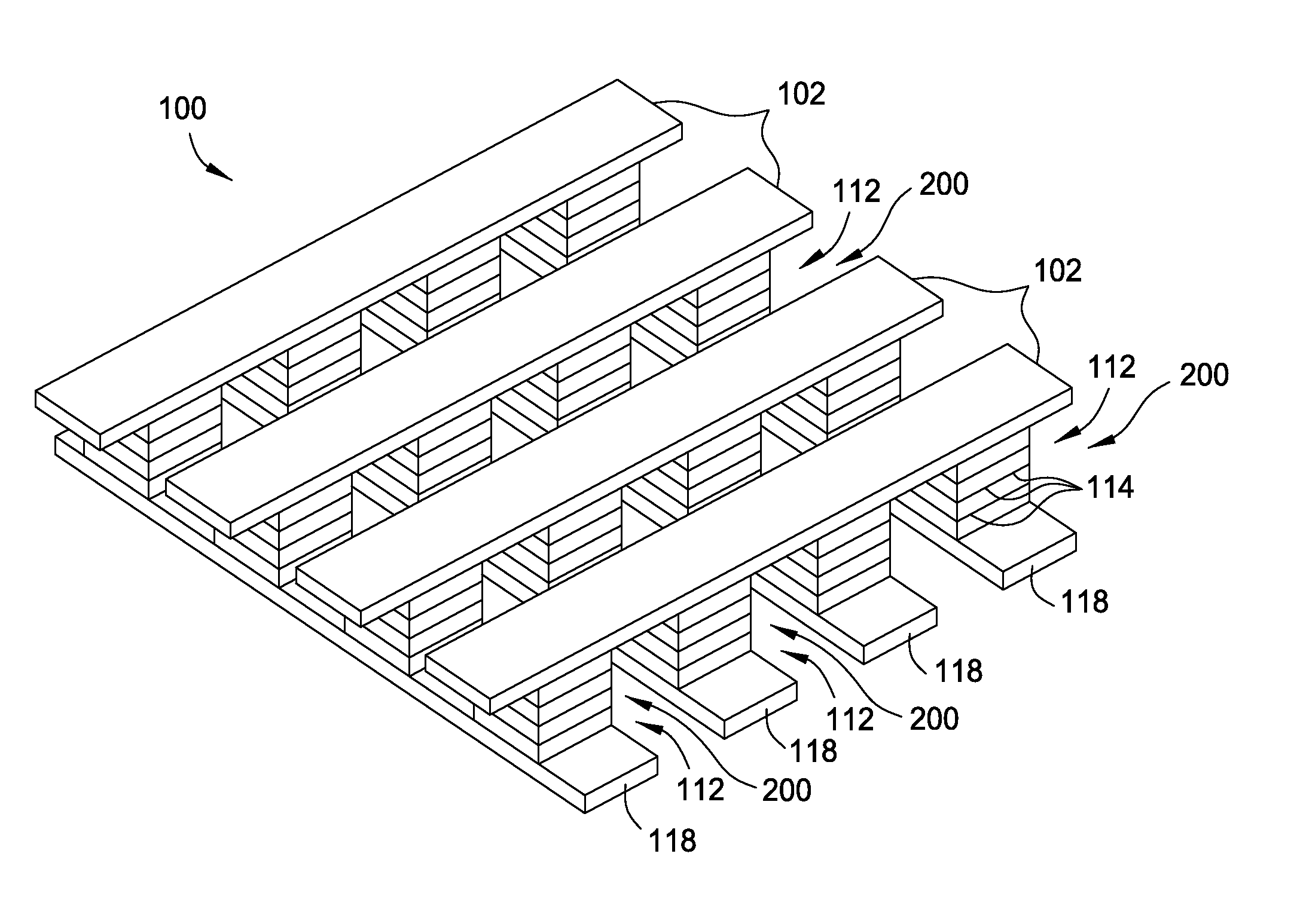
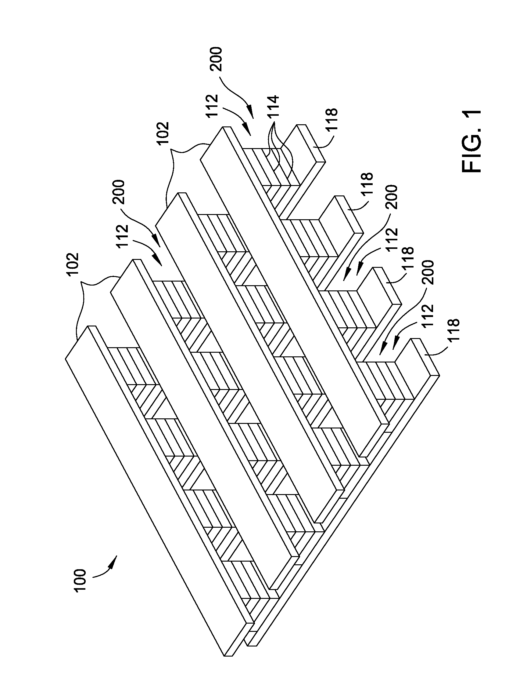
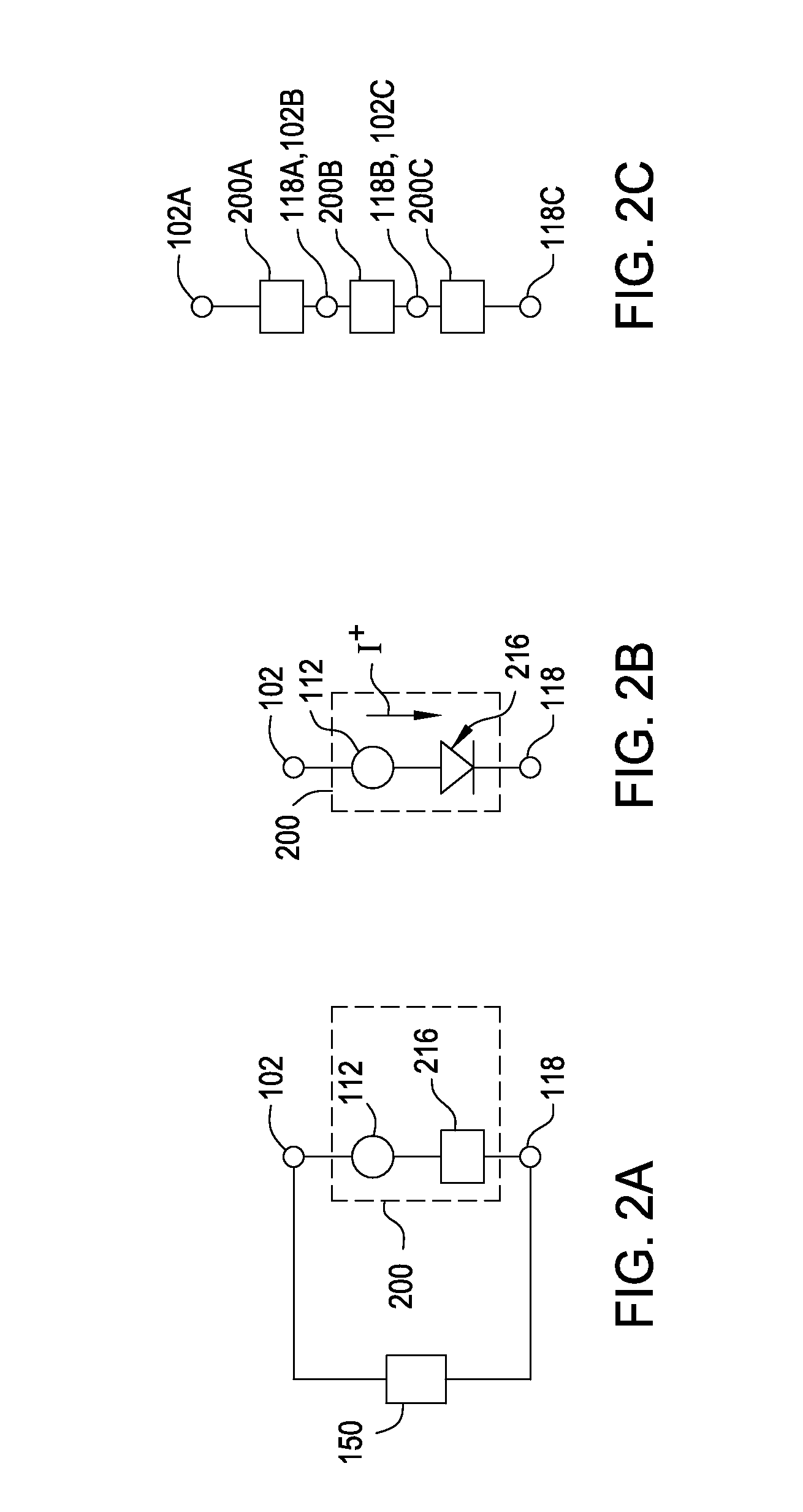
[0034]Embodiments of the present invention generally relate to a resistive switching nonvolatile memory element that is formed in a resistive switching memory device that may be used in a memory array to store digital data. The memory element is generally constructed as a metal-insulator-metal stack. The resistive switching portion of the memory element includes a getter portion and / or a defect portion. In general, the getter portion is an area of the memory element that is used to help form, during the resistive switching memory device's fabrication process, a region of the resistive switching layer that has a greater number of vacancies or defects as compared to the remainder of resistive switching layer. The defect portion is a formed region or area of the memory element that has a greater number of vacancies or defects as compared to the remainder of the resistive switching layer. The addition of the getter or defect portions in a formed memory device generally improves the reli...


PUM


Abstract

Embodiments of the present invention generally relate to a resistive switching nonvolatile memory element that is formed in a resistive switching memory device that may be used in a memory array to store digital data. The memory element is generally constructed as a metal-insulator-metal stack. The resistive switching portion of the memory element includes a getter portion and/or a defect portion. In general, the getter portion is an area of the memory element that is used to help form, during the resistive switching memory device's fabrication process, a region of the resistive switching layer that has a greater number of vacancies or defects as compared to the remainder of resistive switching layer. The defect portion is an area of the memory element that has a greater number of vacancies or defects as compared to the remainder of the resistive switching layer, and is formed during the resistive switching memory device's fabrication process. The addition of the getter or defect portions in a formed memory device generally improves the reliability of the resistive switching memory device, improves the switching characteristics of the formed memory device and can eliminate or reduce the need for the time consuming additional post fabrication “burn-in” or pre-programming steps.

Description

BACKGROUND OF THE INVENTION[0001]1. Field of the Invention[0002]This invention relates to nonvolatile memory elements, and more particularly, to methods for forming resistive switching memory elements used in nonvolatile memory devices.[0003]2. Description of the Related Art[0004]Nonvolatile memory elements are used in systems in which persistent storage is required. For example, digital cameras use nonvolatile memory cards to store images and digital music players use nonvolatile memory to store audio data. Nonvolatile memory is also used to persistently store data in computer environments.[0005]Nonvolatile memory is often formed using electrically-erasable programmable read only memory (EPROM) technology. This type of nonvolatile memory contains floating gate transistors that can be selectively programmed or erased by application of suitable voltages to their terminals.[0006]As fabrication techniques improve, it is becoming possible to fabricate nonvolatile memory elements with in...

Claims


Application Information

Patent Timeline
IPC IPC(8): H01L45/00
CPCH01L45/08H01L45/146H01L45/122H01L27/2463H01L45/1608H10B63/80H10N70/24H10N70/021H10N70/8833H10N70/821
Inventor WANG, YUNCHIANG, TONYHASHIM, IMRAN
Owner KIOXIA CORP
Why Eureka
Try Eureka