
Image Sensor with Reduced Noiseby Blocking Nitridation Over Selected Areas

Inactive Publication Date: 2013-03-07
OMNIVISION TECH INC
View PDF3 Cites 36 Cited by
  • Summary
  • Abstract
  • Description
  • Claims
  • Application Information

AI Technical Summary

Benefits of technology

The patent text discusses a problem in the fabrication of integrated circuits, particularly in the design of optical sensors. As devices become smaller, the amount of charge accumulated by the photodiodes in the sensor arrays becomes smaller, resulting in a decrease in signal-to-noise ratio. One source of noise in the sensor is RTS noise, which arises from defects at interfaces between Si and SiO2 layers. The text proposes a solution to reduce RTS noise by nitriding the gate oxide layers to impede the penetration of boron dopant atoms. However, the nitridation process can also introduce additional noise, including higher RTS noise. The patent text describes various techniques to control the nitridation process and suppress the impact of nitridation on the resulting pixels.

Problems solved by technology

The other areas are filled with insulators, spacers, or gaps that simply cannot be used due to the limitations of a particular layout design or the fabrication equipment.
One source of noise in sensor arrays is RTS (Random Telegraph Signal) noise, although there are other noise sources as well.
RTS noise is caused, at least in part, by defects at interfaces between Si and SiO2 layers in the system.
It is believed that charge carriers are trapped and detrapped at these interface defects.
The noise can cause undesirable flickering pixels and increase the noise of the resulting images.
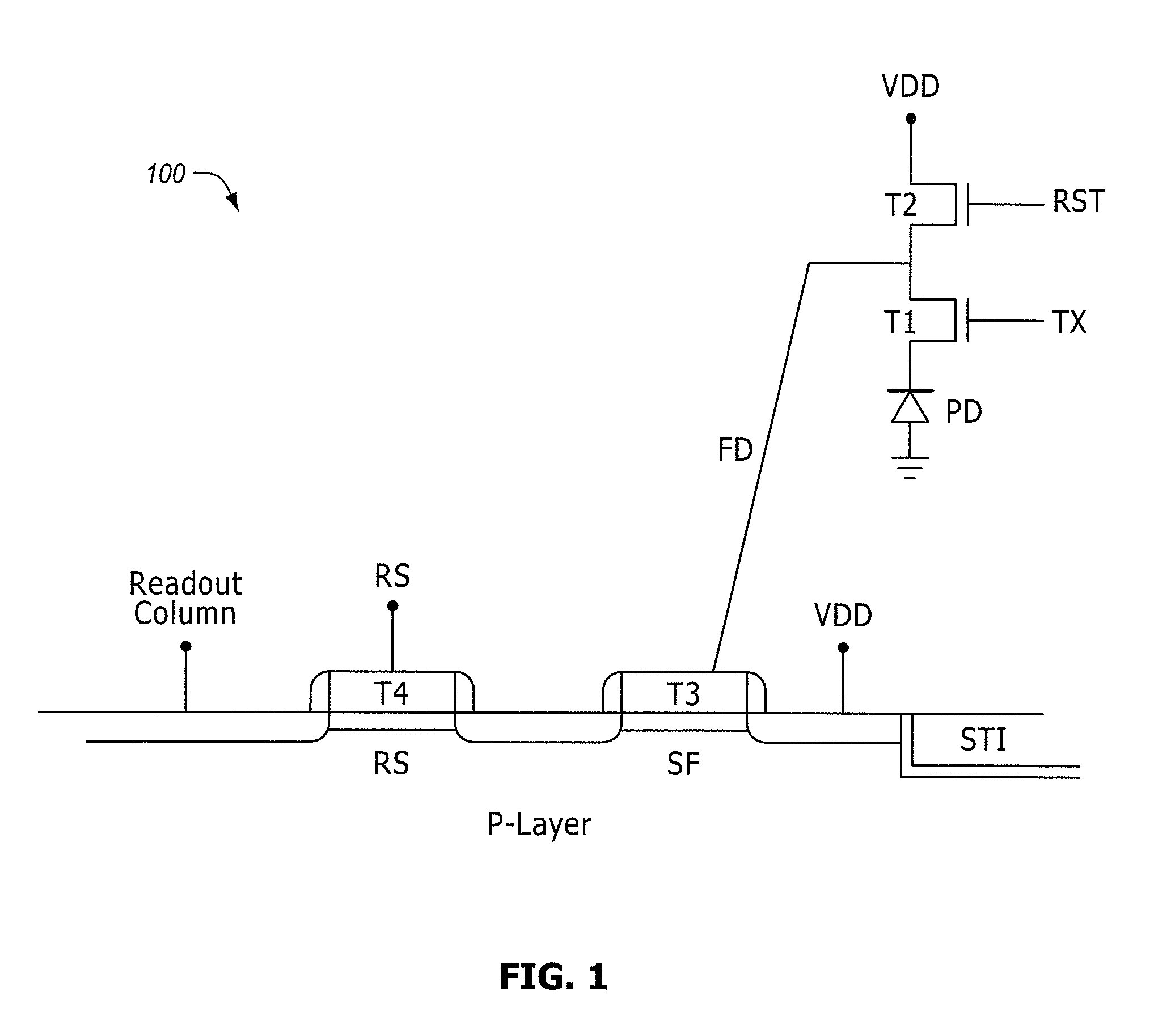
While such noise can cause problems in a variety of devices, it has a noticeable effect with an in-pixel source-follower transistor.
At low light levels, RTS from the source-follower is a significant noise source limiting imaging quality.
This may result in higher RTS noise in an image sensor source-follower transistor as well as in other locations.
DPN also has higher costs because it requires advanced processing tools.

Method used


Image

  • Image Sensor with Reduced Noiseby Blocking Nitridation Over Selected Areas
  • Image Sensor with Reduced Noiseby Blocking Nitridation Over Selected Areas
  • Image Sensor with Reduced Noiseby Blocking Nitridation Over Selected Areas

Examples


Embodiment Construction

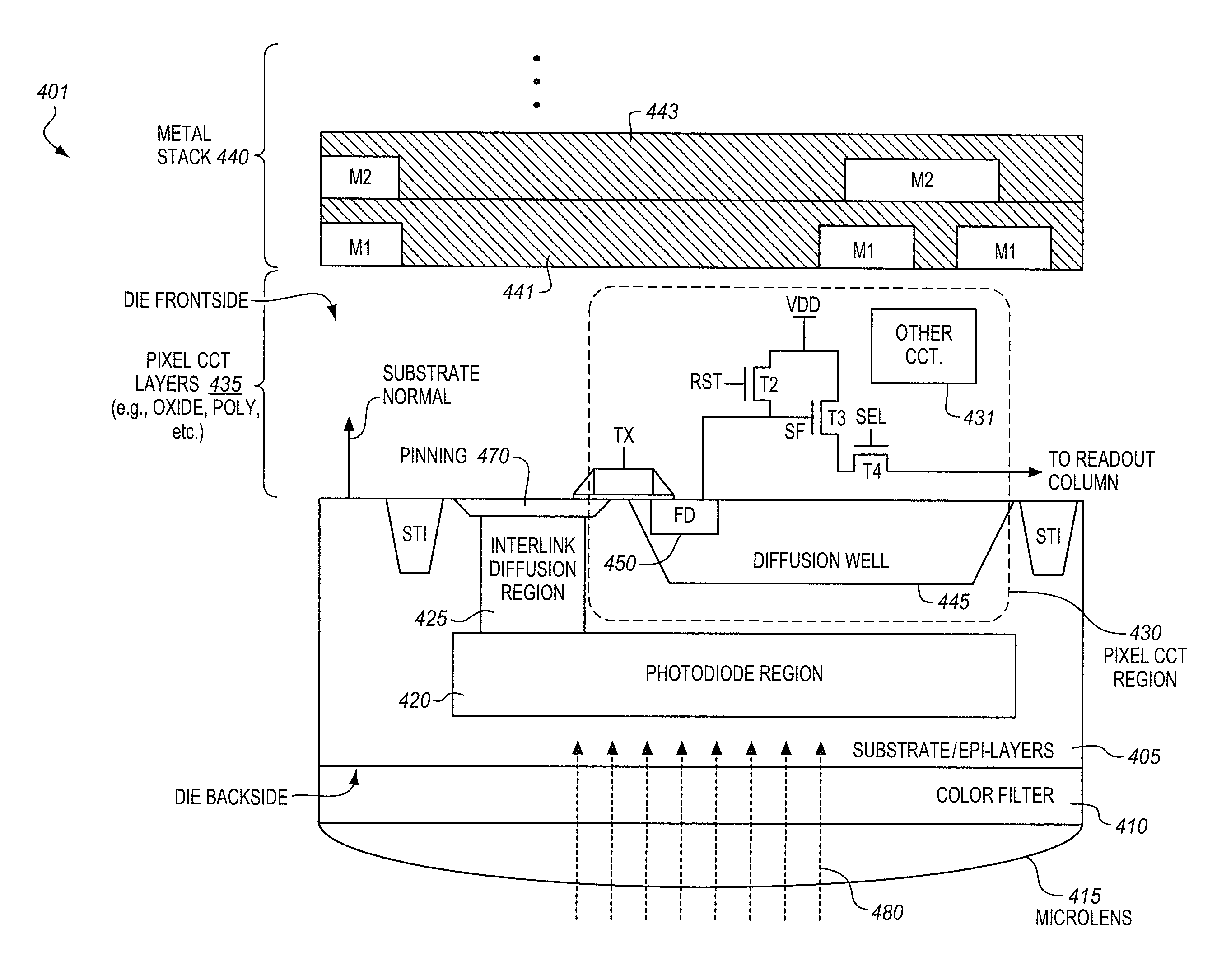
[0013]Typically, a semiconductor has a gate oxide under the gate electrode of any CMOS transistors. The thickness of the gate oxide is adjusted based on the electrical characteristics that are desired for each transistor. In a pixel circuit, a source-follower transistor, which serves as an amplifier, will have a much thicker gate oxide than many of the other transistors that serve as switches. However, when nitridation is used it is typically applied over the whole silicon wafer surface. As a result, both thin and thick gate oxides are subject to nitridation. However, nitridation is only needed to block boron penetration for thin gate oxide layers. Thick gate oxide layers, commonly used for pixel array amplifiers and for analog circuit elements are much less susceptible to boron penetration.

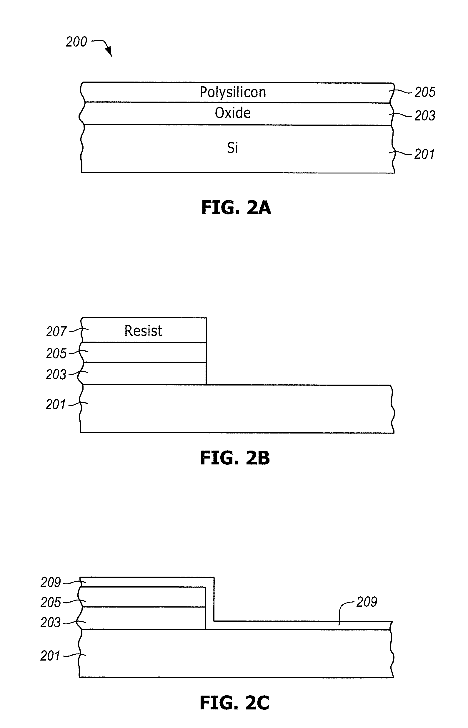
[0014]The source-follower gate oxide layers can be protected from nitridation while the standard gate oxides are exposed to nitridation. A barrier layer can be deposited over the thick gate oxide...


PUM


Abstract

An image sensor is described in which the imaging pixels have reduced noise by blocking nitridation in selected areas. In one example, an imaging pixel of an image sensor includes a photodiode region to accumulate an image charge in response to incident light, a first transistor having a gate oxide layer, the gate oxide layer having a first level of nitridation, and a second transistor having a gate oxide layer, the gate oxide layer having a second level of nitridation that is higher than the first level of nitridation.

Description

TECHNICAL FIELD[0001]The present disclosure relates generally to integrated circuits, and more particularly, to the protection of transistor gate oxide areas during nitridation.BACKGROUND INFORMATION[0002]In an integrated circuit, designers seek to increase the circuit density. In other words, designers seek to place more electronic devices in the same amount of space. The active devices are located in what is referred to active areas. The other areas are filled with insulators, spacers, or gaps that simply cannot be used due to the limitations of a particular layout design or the fabrication equipment.[0003]In optical sensors, designers seek to increase the amount of space used for photodiodes (or any other type of optical sensor) as compared to other devices. This allows for larger photosites or for more photosites in the same amount of space, increasing the quality of the sensor output, or decreasing the total size of the sensor with the same quality, or both. For an optical sens...

Claims


Application Information

Patent Timeline
IPC IPC(8): H01L31/113H01L31/18
CPCH01L27/14614H01L27/14689H01L27/1464
Inventor MAO, DULITAI, HSIN CHIHVENEZIA, VINCENTRHODES, HOWARD
Owner OMNIVISION TECH INC
Learn More