Methods for fabricating integrated circuits

a technology of integrated circuits and manufacturing methods, applied in the direction of basic electric elements, electrical equipment, semiconductor devices, etc., can solve the problems of reducing device size, reducing feature size, and fabrication problems

Active Publication Date: 2013-03-14
GLOBALFOUNDRIES INC
View PDF1 Cites 176 Cited by
  • Summary
  • Abstract
  • Description
  • Claims
  • Application Information

AI Technical Summary

Benefits of technology

[0009]In accordance with yet another embodiment a method for fabricating a silicon integrated circuit includes forming shallow trench isolation to define an area of a silicon substrate. Dummy gate structures are formed overlying the area and defining a channel in the area. Sidewall spacers are formed on the dummy gate structures and spin on glass material is deposited between the dummy gate structures. The dummy gate structures are removed using the spin on glass material

Problems solved by technology

Even with FINFETs, however, reducing device size and hence reducing feature size introduces fabrication problems.
Such problems include adverse short channel effects as the gate length shrinks and the attendant variation in threshold voltage (basically the minimum gate voltage necessary to turn a transistor “ON”) from random dopant fluctuations in the channel.
Threshold variations, in turn, lead to problems with unmatched transistors.
One solution is to fabric

Method used


Image

  • Methods for fabricating integrated circuits
  • Methods for fabricating integrated circuits
  • Methods for fabricating integrated circuits

Examples


Embodiment Construction

[0015]The following detailed description is merely exemplary in nature and is not intended to limit the invention or the application and uses of the invention. Furthermore, there is no intention to be bound by any expressed or implied theory presented in the preceding technical field, background, brief summary or the following detailed description.

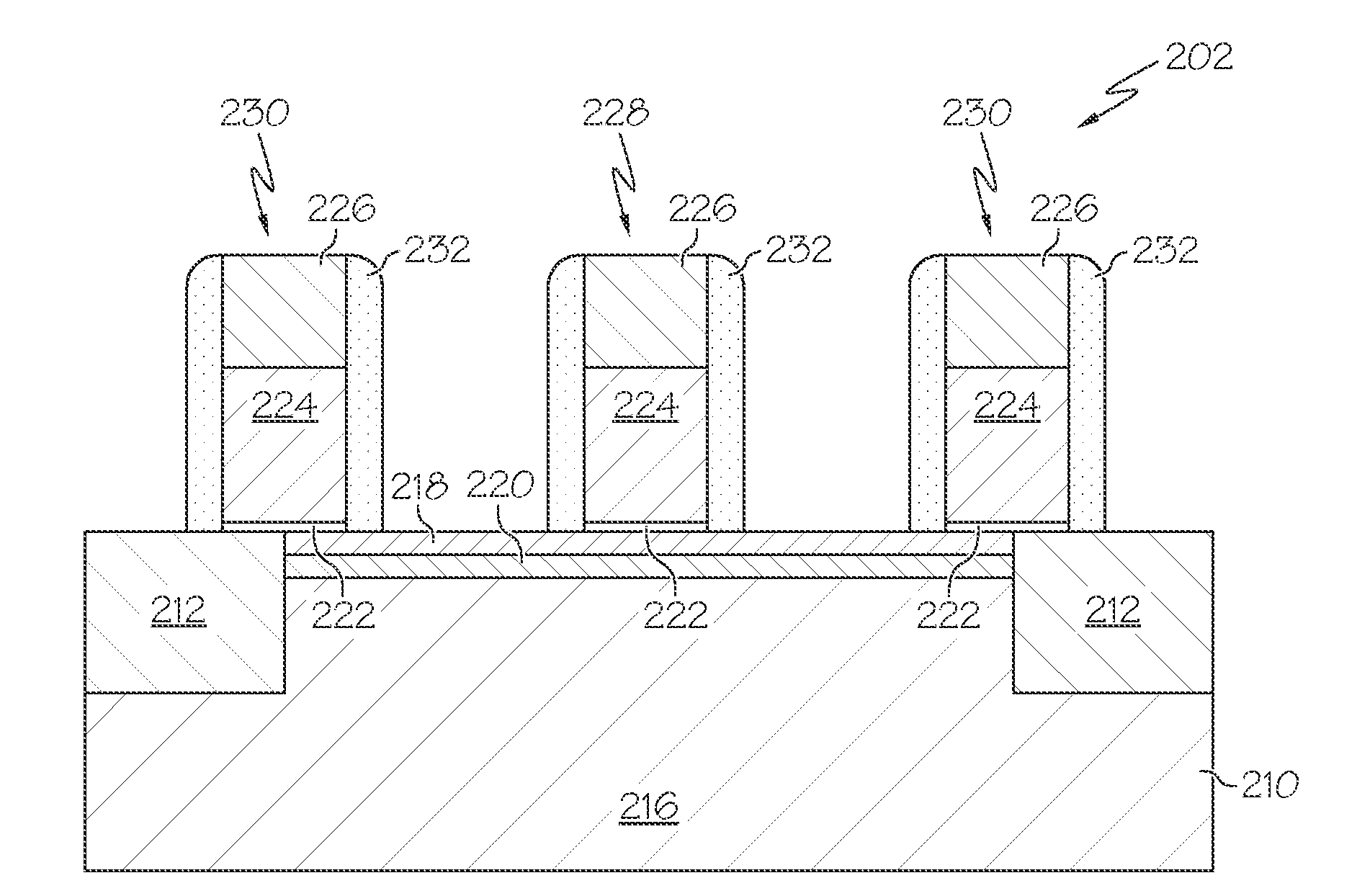
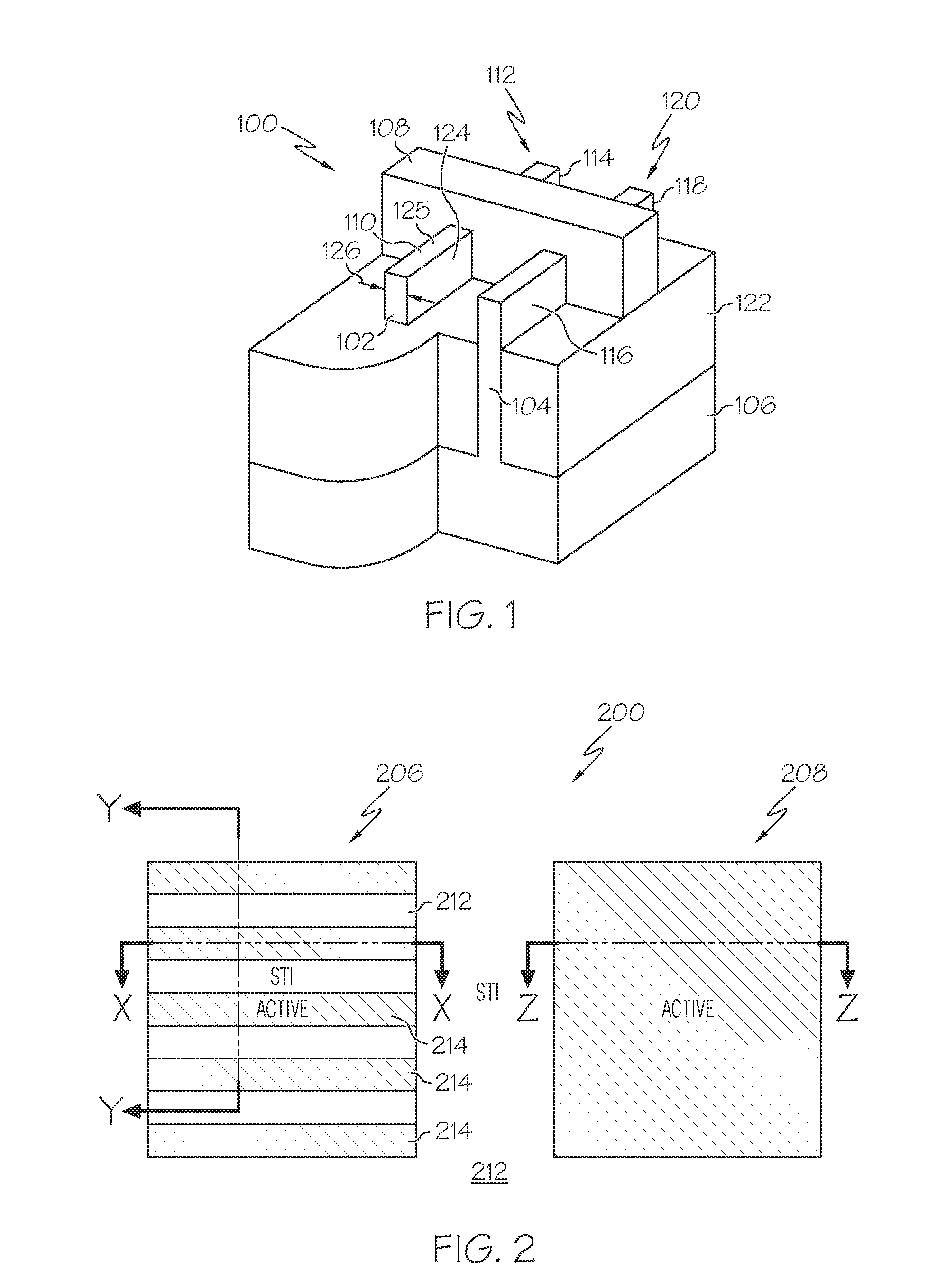
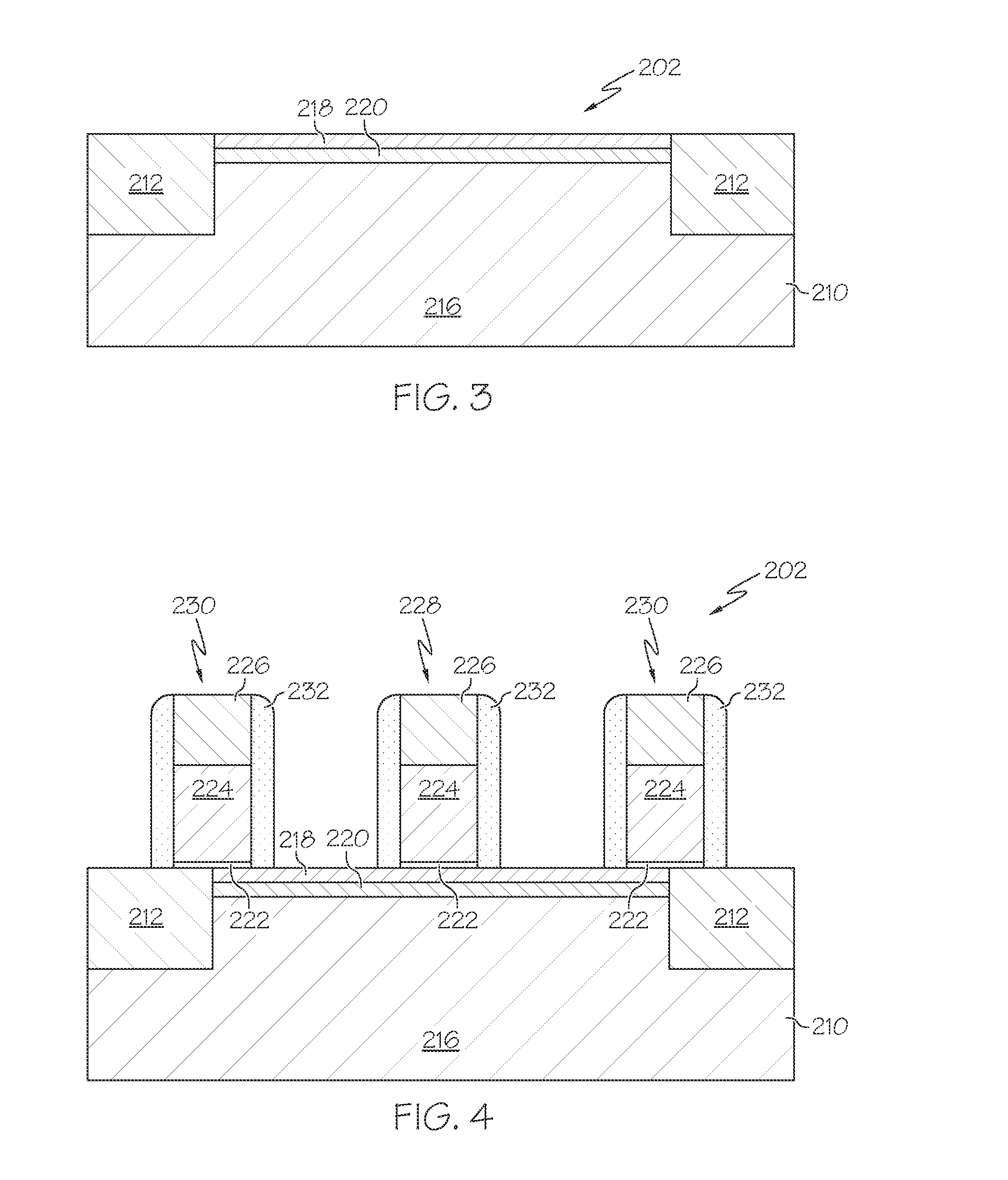
[0016]Integrated circuits (ICs) can be designed with millions of transistors. Many ICs are designed using metal oxide semiconductor (MOS) transistors, also known as field effect transistors (FETs) or MOSFETs. Although the term “MOS transistor” properly refers to a device having a metal gate electrode and an oxide gate insulator, that term will be used throughout to refer to any semiconductor device that includes a conductive gate electrode (whether metal or other conductive material) that is positioned over a gate insulator (whether oxide or other insulator) which, in turn, is positioned over a semiconductor substrate. MOS transistors used...


PUM


Abstract

Methods are provided for fabricating integrated circuits. One method includes etching a plurality of trenches into a silicon substrate and filling the trenches with an insulating material to delineate a plurality of spaced apart silicon fins. A layer of undoped silicon is epitaxially grown to form an upper, undoped region of the fins. Dummy gate structures are formed overlying and transverse to the plurality of fins and a back fill material fills between the dummy gate structures. The dummy gate structures are removed to expose a portion of the fins and a high-k dielectric material and a work function determining gate electrode material are deposited overlying the portion of the fins. The back fill material is removed to expose a second portion and metal silicide contacts are formed on the second portion. Conductive contacts are then formed to the work function determining material and to the metal silicide.

Description

TECHNICAL FIELD[0001]The present invention generally relates to methods for fabricating integrated circuits, and more particularly relates to methods for fabricating integrated circuits having undoped channel regions and self aligned contacts.BACKGROUND[0002]Transistors such as metal oxide semiconductor field effect transistors (MOSFETs) or simply field effect transistors (FETs) or MOS transistors are the core building blocks of the vast majority of semiconductor integrated circuits (ICs). A FET includes source and drain regions between which a current can flow through a channel under the influence of a bias applied to a gate electrode that overlies the channel. Some semiconductor ICs, such as high performance microprocessors, can include millions of FETs. For such ICs, decreasing transistor size and thus increasing transistor density has traditionally been a high priority in the semiconductor manufacturing industry. Transistor performance, however, must be maintained even as the tr...

Claims


Application Information

Patent Timeline
IPC IPC(8): H01L21/336H01L21/762H01L21/20
CPCH01L21/76224H01L21/823821H01L29/66545H01L21/76897H01L21/823431H01L29/66636H01L29/7848H01L21/823418H01L29/41783
Inventor WEI, ANDY C.BAARS, PETERGEISS, ERIK P.
Owner GLOBALFOUNDRIES INC
Why Eureka
Try Eureka