Shift register circuit

a register circuit and shift register technology, applied in logic circuits, digital storage, instruments, etc., can solve the problems of increased layout area, increased power consumption, depletion of transistors, etc., and achieve the effect of reducing manufacturing costs

Inactive Publication Date: 2013-03-28
SEMICON ENERGY LAB CO LTD
View PDF5 Cites 11 Cited by
  • Summary
  • Abstract
  • Description
  • Claims
  • Application Information

AI Technical Summary

Benefits of technology

[0007]In a driver circuit including transistors having one conductivity type, a doping step or the like in a manufacturing process of the transistors can be skipped un

Problems solved by technology

As a result, there is a problem in that the layout area is increased.
On the other hand, when a driver circuit including transistors having the same conductivity type is formed, there is a problem in that both a depletion transistor (also referred to as normally-on transistor) and an enhancement transistor (also referred to as normally-off transistor) are provided due to a shift in threshold voltage of the transistors.
Since t

Method used


Image

  • Shift register circuit
  • Shift register circuit
  • Shift register circuit

Examples


embodiment 1

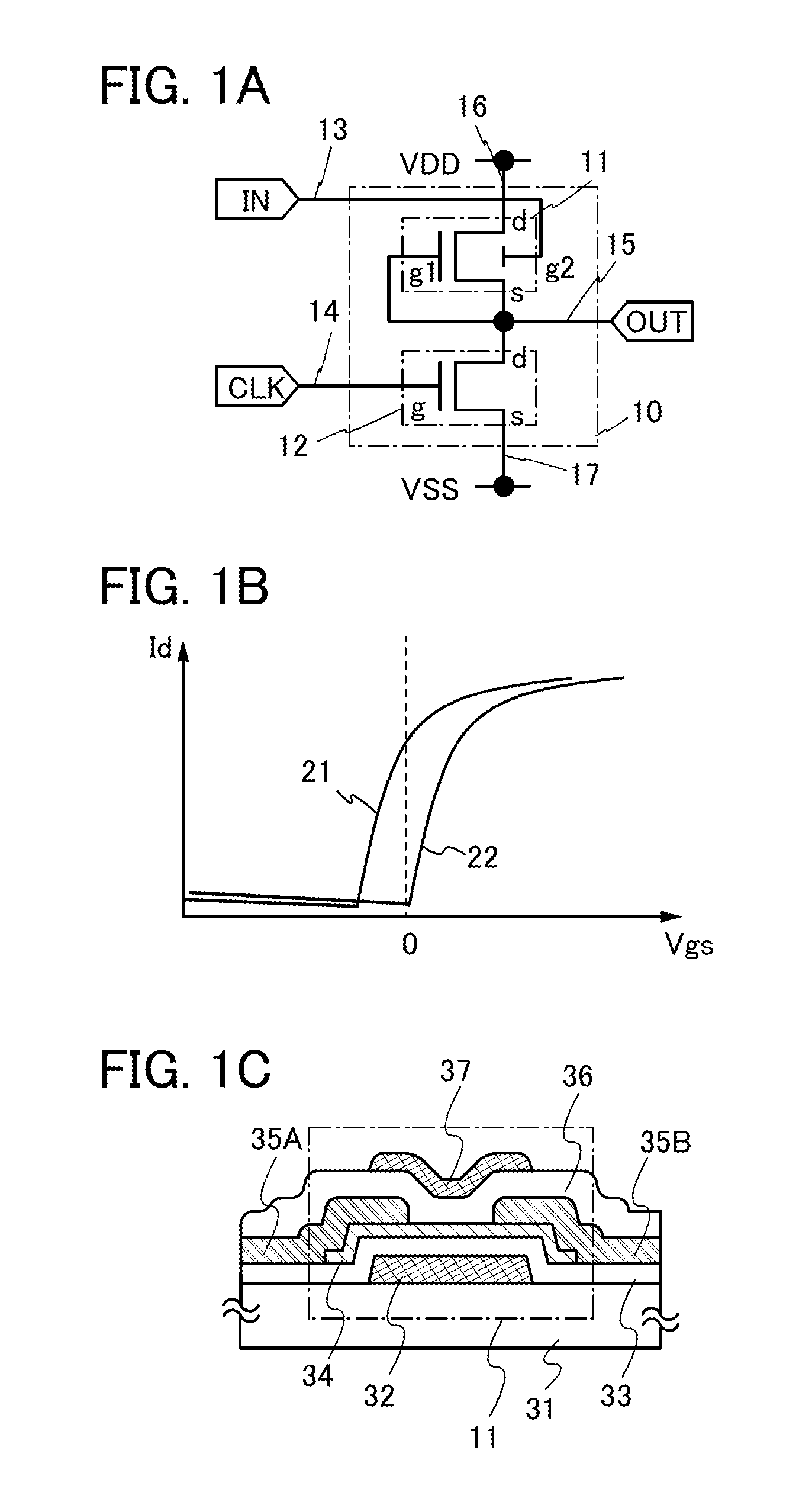
[0032]First, a configuration of a logic circuit which is provided in a shift register circuit and includes a first transistor and a second transistor will be described.

[0033]A logic circuit 10 illustrated in FIG. 1A includes a first transistor 11 and a second transistor 12.

[0034]Although each of the first transistor 11 and the second transistor 12 is described in this embodiment as being an n-channel transistor, each of the first transistor 11 and the second transistor 12 may be a p-channel transistor.

[0035]In the first transistor 11 of FIG. 1A, a first gate electrode, a source electrode, a drain electrode, and a second gate electrode are illustrated with shortened names, g1, s, d, and g2, respectively. The first gate electrode of the first transistor 11 is connected to the source electrode of the first transistor 11. The second gate electrode of the first transistor 11 is connected to a wiring 13. The drain electrode of the first transistor 11 is connected to a wiring 16.

[0036]In t...

embodiment 2

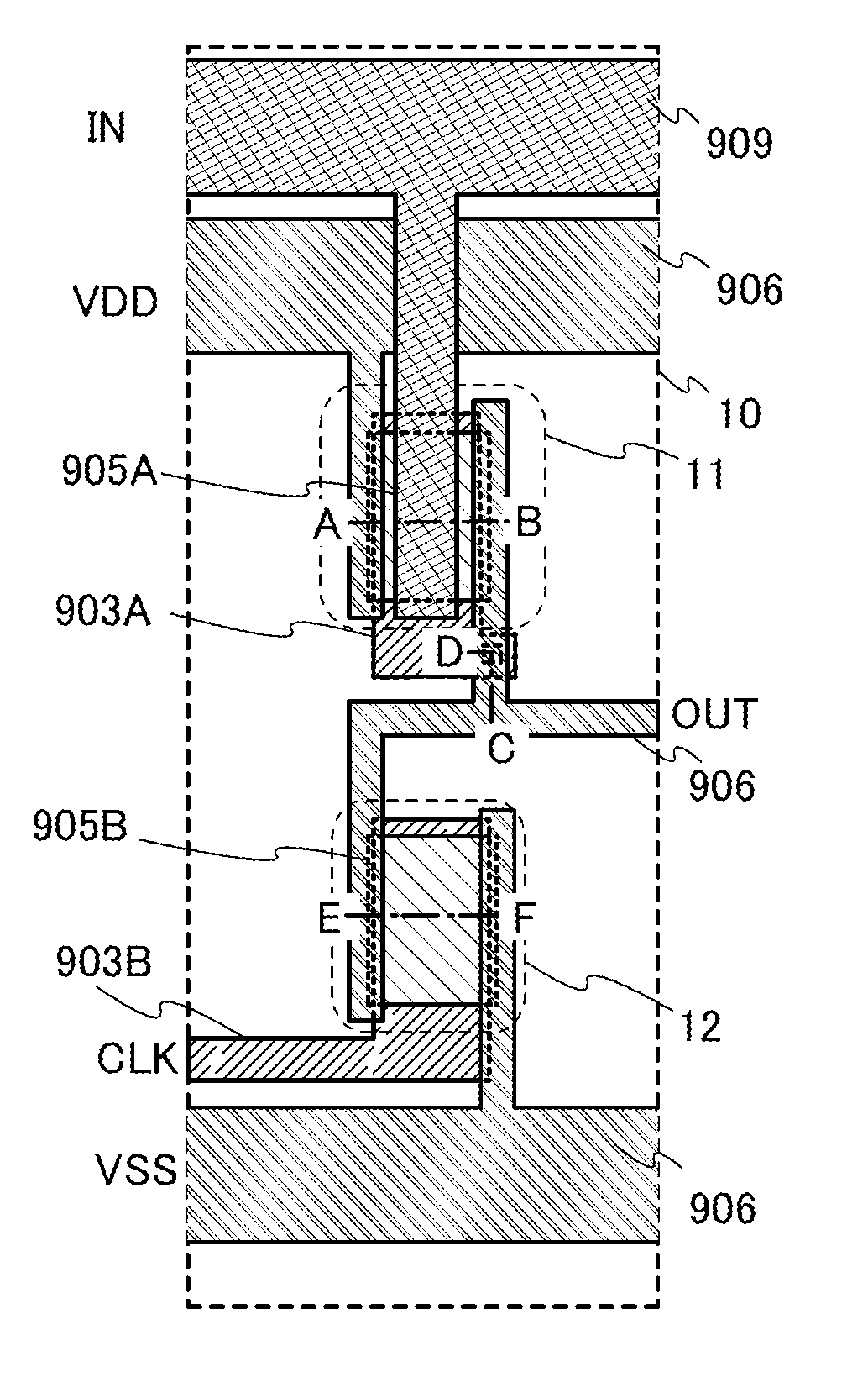
[0084]In this embodiment, a top view and a cross-sectional view of the shift register circuit described in the above embodiment will be described; particularly, a top view and a cross-sectional view of the first transistor and the second transistor included in the logic circuit will be described. Note that a display device including a shift register circuit in this embodiment can be applied to a liquid crystal display device and a display device including a light-emitting element such as an organic EL element. The shift register circuit described in the above embodiment can be employed as a driver circuit of an electronic paper including an electrophoresis element. Note that the shift register circuit described in the above embodiment can be applied to not only a driver circuit of a display device but also other devices such as a driver circuit for a photosensor.

[0085]FIG. 5 is a top view of the logic circuit 10 including the first transistor 11 and the second transistor 12 describe...

embodiment 3

[0103]In this embodiment, an example of providing, over the same substrate, a transistor to be disposed in a pixel portion, and part of a signal line driver circuit and / or a scan line driver circuit including a shift register circuit will be described below.

[0104]FIG. 7A is an example of a block diagram of an active matrix display device. A pixel portion 5301, a first scan line driver circuit 5302, a second scan line driver circuit 5303, and a signal line driver circuit 5304 are formed over a substrate 5300 of the display device. A plurality of signal lines extended from the signal line driver circuit 5304 and a plurality of scan lines extended from the first scan line driver circuit 5302 and the second scan line driver circuit 5303 are provided in the pixel portion 5301. Note that pixels each including a display element are arranged in a matrix in respective regions where the scan lines and the signal lines intersect with each other. The substrate 5300 of the display device is conn...


PUM


Abstract

A shift register circuit including a logic circuit capable of controlling the threshold voltage of a transistor and outputting a signal corresponding to an input signal by changing only the potential of a back gate without changing the potential of a gate is provided. In a shift register circuit including a logic circuit with a first transistor and a second transistor having the same conductivity type, a first gate electrode of the first transistor is connected to a source electrode or a drain electrode of the first transistor, an input signal is supplied to a second gate electrode of the first transistor, a clock signal is supplied to a gate electrode of the second transistor, and the first gate electrode and the gate electrode are formed from the same layer.

Description

BACKGROUND OF THE INVENTION[0001]1. Field of the Invention[0002]The present invention relates to a shift register circuit. Further, the present invention relates to a display device in which a shift register circuit is formed over the same substrate as a pixel portion. Furthermore, the present invention relates to an electronic device including the display device.[0003]2. Description of the Related Art[0004]Display devices such as liquid crystal televisions are required to be manufactured at lower cost so as to be more widely used, so that development thereof have been conducted. In particular, a technique in which a driver circuit such as a scan line driver circuit is formed using a thin film transistor (TFT) over the same substrate as a pixel portion has been actively developed.[0005]As an example of a driver circuit that can be formed over the same substrate as a pixel portion, there is a driver circuit having a configuration in which transistors having the same conductivity type...

Claims


Application Information

Patent Timeline
IPC IPC(8): H01L25/00G11C19/00
CPCG11C19/28G09G3/36
Inventor HIROSE, ATSUSHI
Owner SEMICON ENERGY LAB CO LTD
Why Eureka
Try Eureka