

Circuit pattern inspection apparatus and circuit pattern inspection method
a circuit pattern inspection and circuit pattern technology, applied in the direction of material analysis using wave/particle radiation, instruments, image enhancement, etc., can solve the problems of reducing the throughput, reducing the detection speed and high-resolution imaging, and reducing the performance of defect detection smaller than the pixel size, so as to reduce the time required for image acquisition and inspection. , the effect of reducing the time required
- Summary
- Abstract
- Description
- Claims
- Application Information
AI Technical Summary
Benefits of technology
Problems solved by technology
Method used
Image

Examples
first embodiment
[0037]A first embodiment will be described below in detail with reference to the drawings.
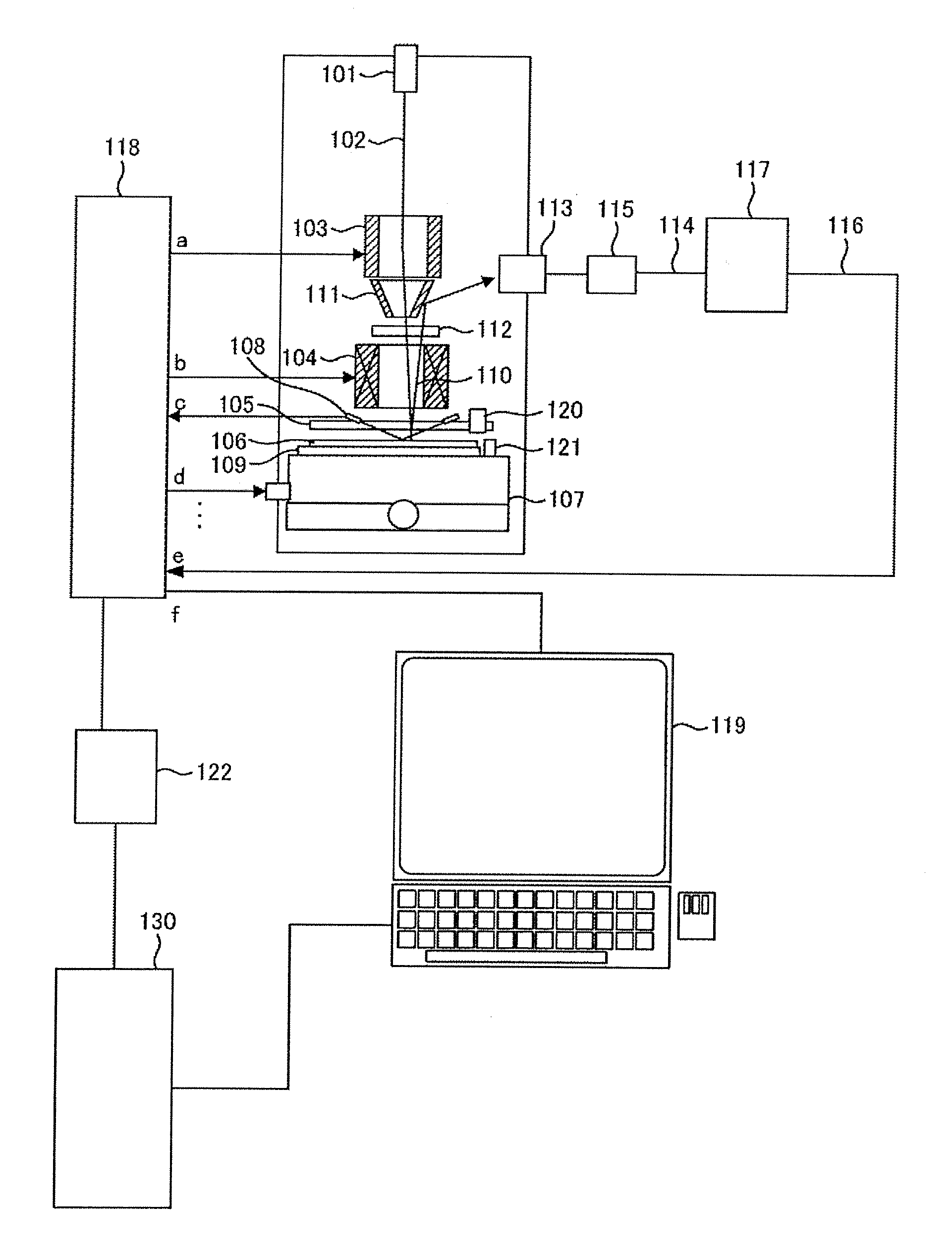
[0038]FIG. 2 is a longitudinal cross-sectional view showing the configuration of an inspection apparatus according to the present embodiment. The inspection apparatus according to the present embodiment is a variation of a scanning electron microscope, and a key portion of the apparatus is accommodated in a vacuum chamber. The reason for this is to irradiate a semiconductor wafer or any other substrate with a primary charged particle beam. The inspection apparatus according to the present embodiment is formed, for example, of a charged particle column in which a primary charged particle beam 102 emitted from an electron source 101 irradiates a wafer 106 placed on a sample table 109 and a detector 113 detects resultant secondary charged particles 110, such as secondary electrons or reflected electrons, and outputs the detected particles as a secondary charged particle signal; an XY stage 107 tha...
second embodiment
[0088]A second embodiment of the invention will be described with reference to FIGS. 13 and 14. The configuration of an apparatus according to the second embodiment is the same as that of the apparatus according to the first embodiment and only differs therefrom, for example, in terms of the stage drive method, and only different portions will therefore be described.
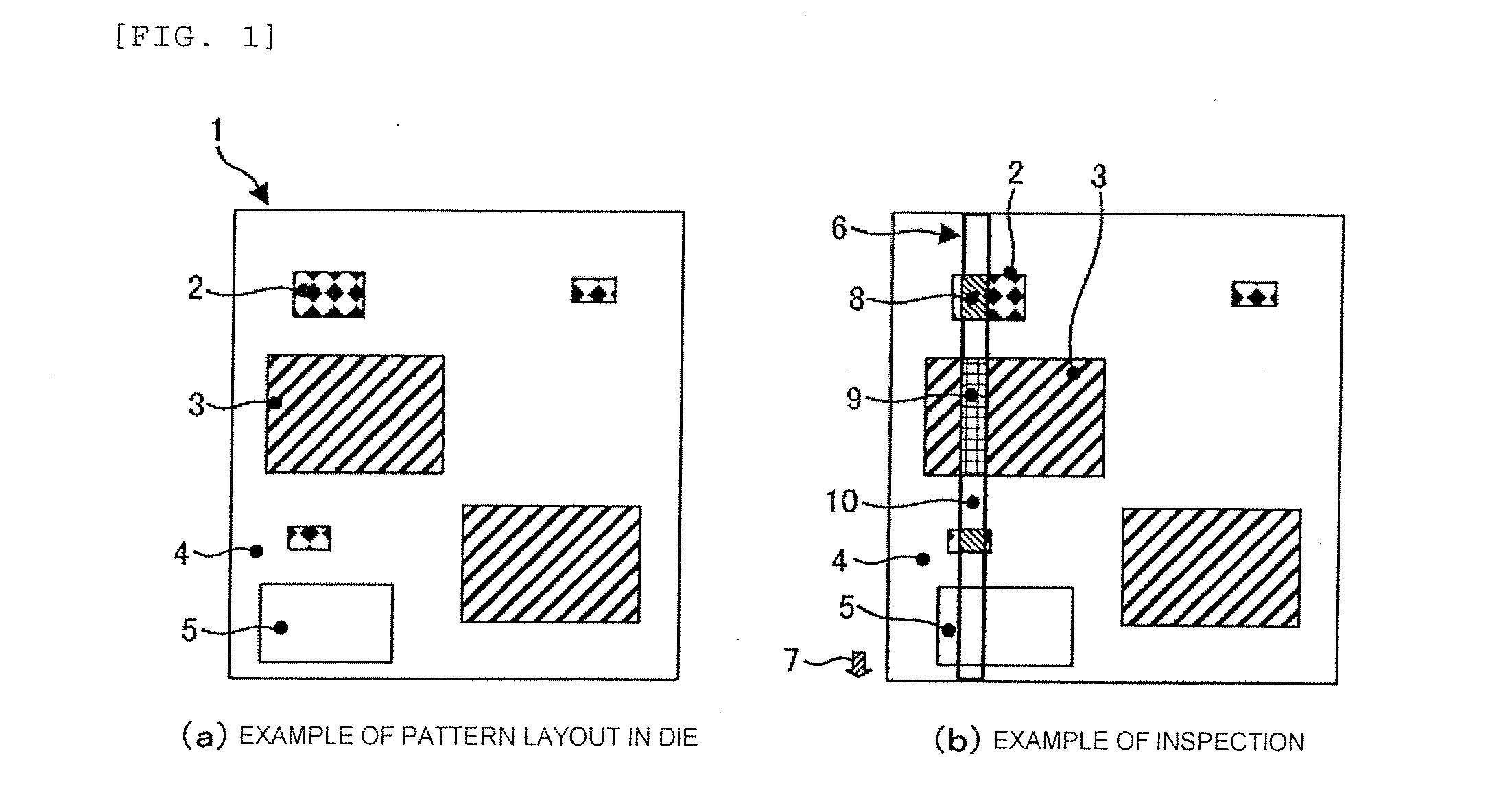
[0089]FIG. 13 describes an example of the layout on a device to be inspected in the second embodiment. FIG. 13(a), a left portion of FIG. 13, is a schematic view showing the layout on an actual object under inspection, and FIG. 13(b), a right portion of FIG. 13, is a schematic view showing a stripe disposed on the object under inspection. A die 1 is formed of a high-density region 2, a middle-density region 3, and a region not to be inspected 5. Consider now that the portion corresponding to a stripe 6 is inspected, that is, a case where the high-density region 2 occupies a large part of the stripe 6 and the middle-densi...
third embodiment
[0096]A third embodiment will next be described with reference to FIG. 15. FIG. 15 shows the configuration of an apparatus according to the third embodiment, which is an example of an optical inspection apparatus. A laser light source 1401 emits laser light 1402 (corresponding to primary charged particle beam 102), which is scanned by a polygonal mirror 1403 (corresponding to X-direction scanning performed by deflector 103), and the amount of scan delay in the Y direction (corresponding to Y-direction scanning performed by deflector 103) is adjusted by a galvanometric mirror 1404. The laser light 1402 then irradiates a wafer 106 via an objective lens 1405. The resultant scattered light is detected by a detector (sensor) 113. The energizing adjustment made on the objective lens is replaced with a Z stage 1406 driven, for example, by a piezoelectric device. The same operation as that in the first or second embodiment is achieved by replacing the operation of the corresponding portions...
PUM
 Abstract
Description
Claims
Application Information