Switching power supply device, and inverter, converter, air conditioner, solar power controller, and automobile employing same

a power supply device and switching technology, applied in the direction of instruments, process and machine control, lighting and heating apparatus, etc., can solve the problems of large switching loss, high cost, and generation of conduction loss in the backflow prevention diode, and achieve high efficiency

Active Publication Date: 2013-04-04
SHARP KK
View PDF12 Cites 16 Cited by
  • Summary
  • Abstract
  • Description
  • Claims
  • Application Information

AI Technical Summary

Benefits of technology

[0009]Accordingly, it is a principal object of the present invention to offer a highly efficient, low-cost switching pow

Problems solved by technology

In such cases, when electrical current flows back in the forward direction to the parasitic diode, and a power supply voltage is applied in the reverse direction to the parasitic diode, recovery current (reverse recovery current) flows to the parasitic diode, generating a large switching loss.
However, a problem encoun

Method used


Image

  • Switching power supply device, and inverter, converter, air conditioner, solar power controller, and automobile employing same
  • Switching power supply device, and inverter, converter, air conditioner, solar power controller, and automobile employing same
  • Switching power supply device, and inverter, converter, air conditioner, solar power controller, and automobile employing same

Examples


first embodiment

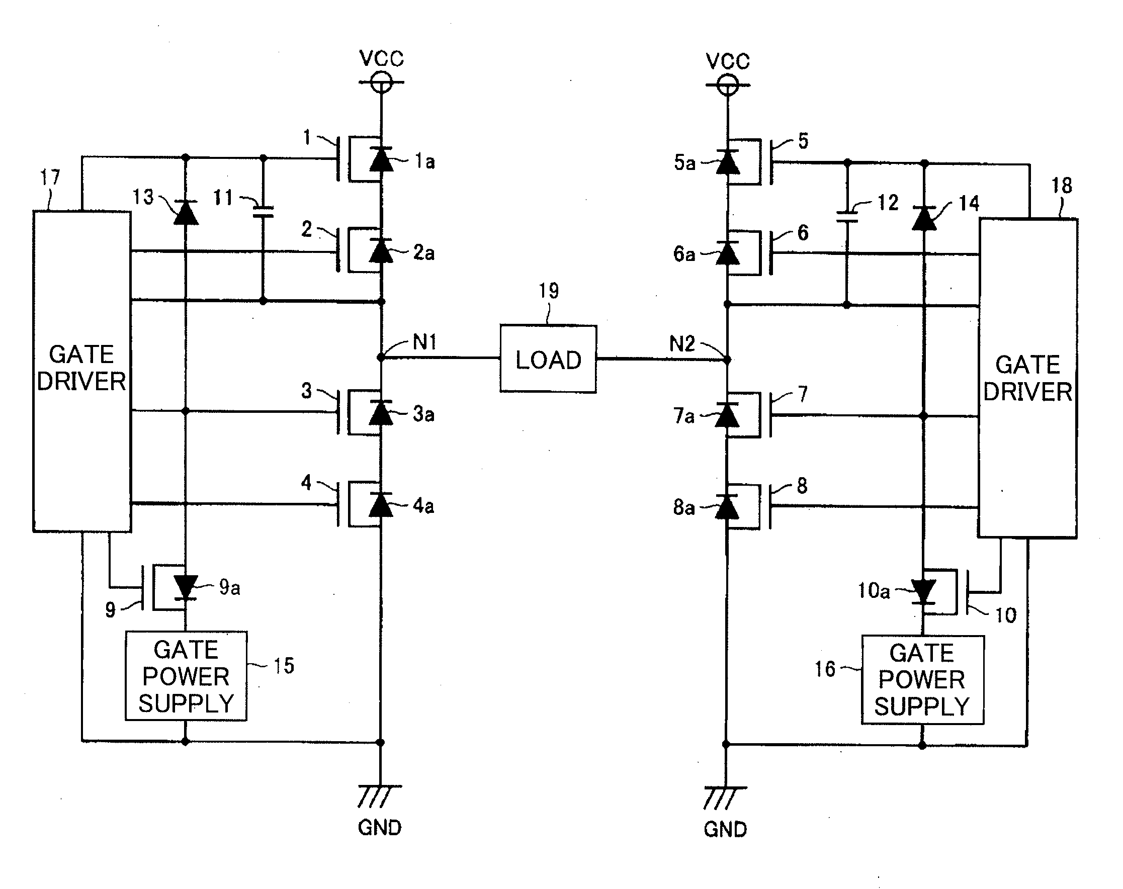
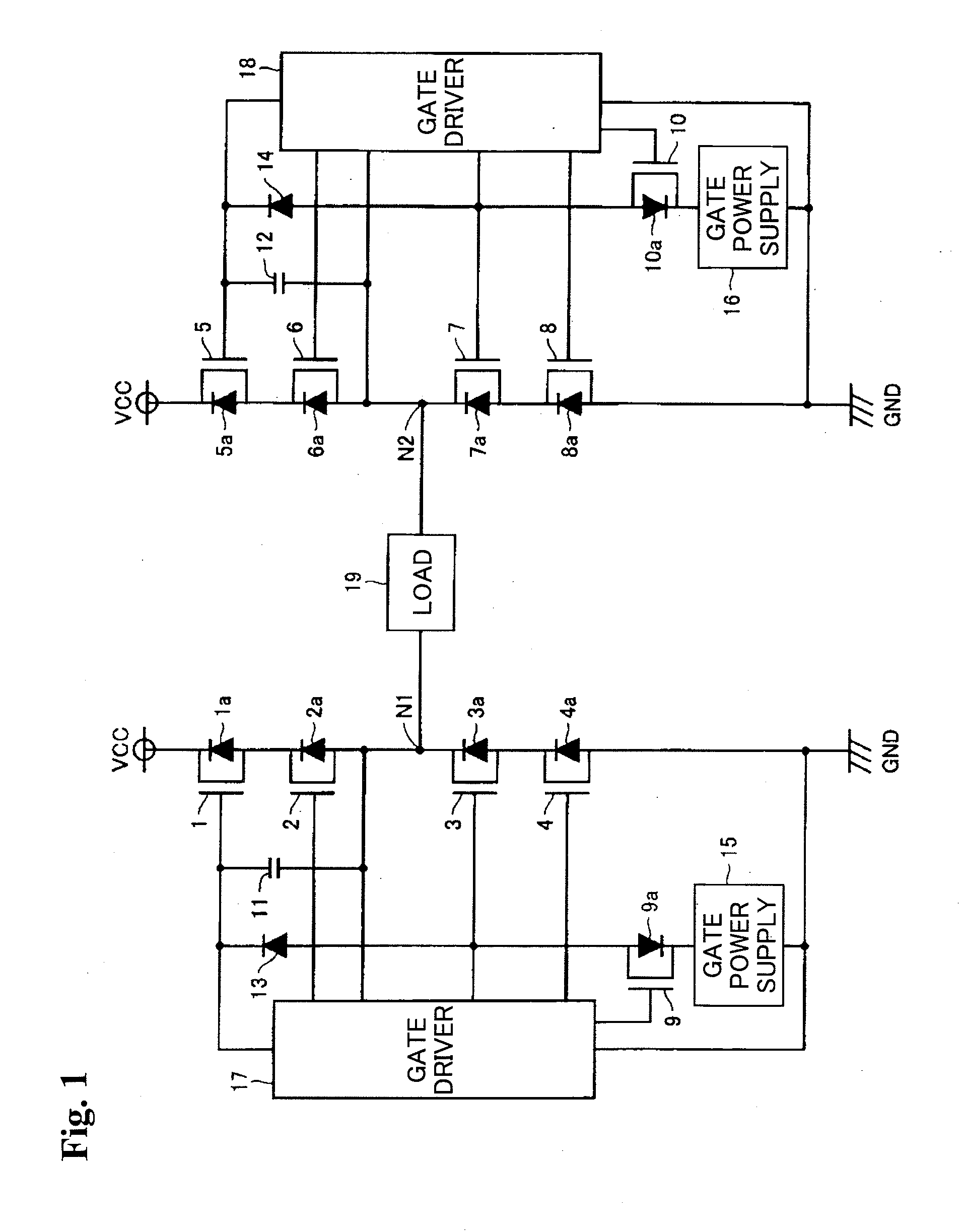
[0037]As shown in FIG. 1, the inverter according to a first embodiment of the present invention is provided with N-channel MOS transistors 1 to 10, capacitors 11 and 12, diodes 13 and 14, gate power supplies 15 and 16, and gate drivers 17 and 18. The transistors 1 to 10 respectively incorporate parasitic diodes 1a to 10a.

[0038]The anodes of the parasitic diodes 1a to 10a are respectively connected to the sources of the corresponding transistors 1 to 10, while the cathodes of the parasitic diodes 1a to 10a are respectively connected to the drains of the corresponding transistors 1 to 10.

[0039]Each of the transistors 1, 3, 5, and 7 is a high-withstand-voltage transistor in which the source-drain withstand voltage is 600 V, for example. Each of the transistors 2, 4, 6, and 8 is a low-withstand-voltage transistor in which the source-drain withstand voltage is 30 V, for example. Typically, the recovery current of the low-withstand-voltage transistors 2, 4, 6, and 8 is lower than the rec...

second embodiment

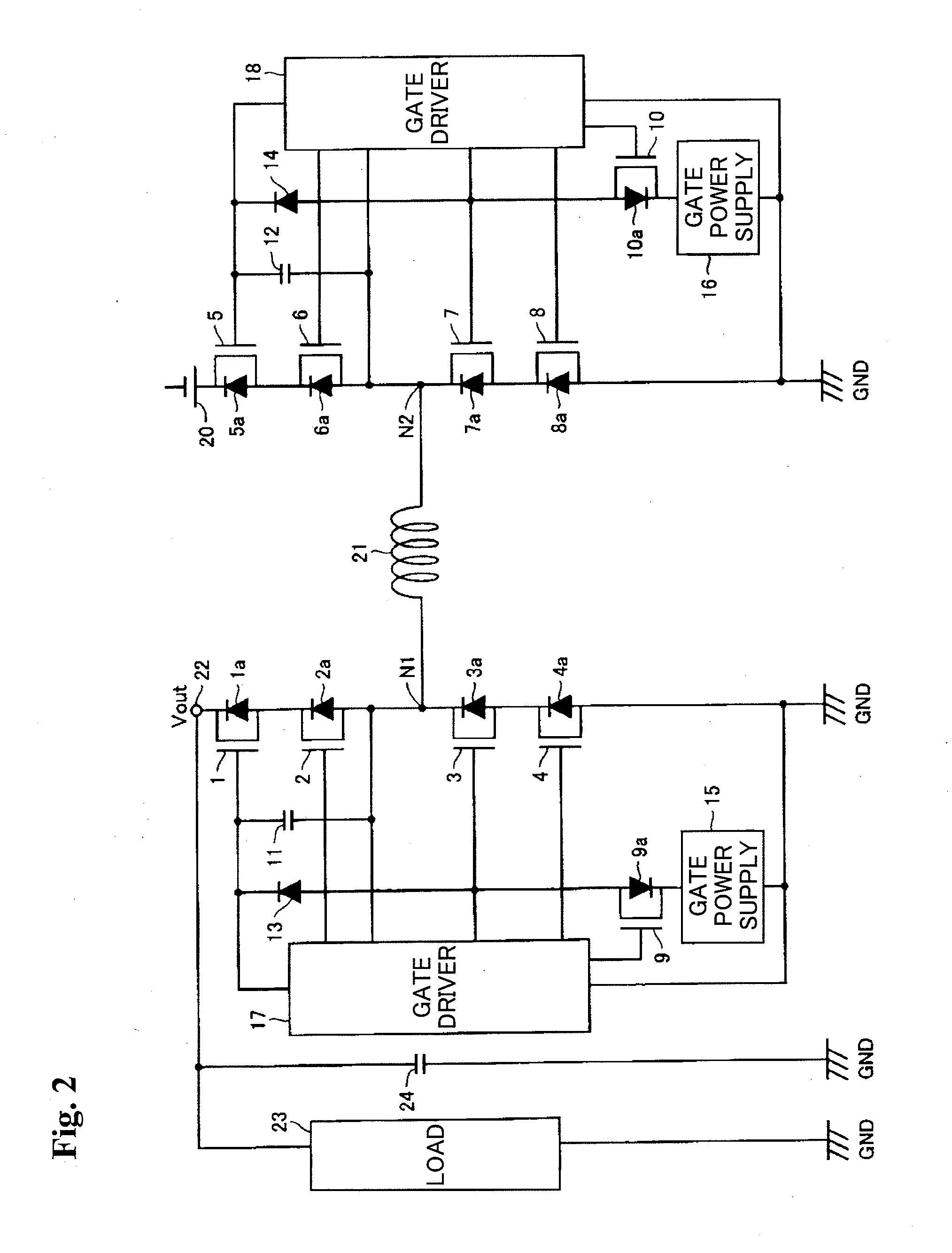
[0078]FIG. 5 is a circuit block diagram showing a configuration of a bidirectional chopper according to a second embodiment of this invention, and the diagram is intended for comparison with FIG. 2. In FIG. 5, bidirectional chopper is provided with the transistors 5 to 8, the capacitor 12, the diode 14, the gate power supply 16, the gate driver 18, and the coil 21 of the circuit of FIG. 2, as well as with diodes 30 to 35, capacitors 36 and 37, and input / output terminals T1 and T2.

[0079]The high-withstand-voltage transistor 5 and the low-withstand-voltage transistor 6 are serially connected between the input / output terminal T2 and the node N2. The high-withstand-voltage transistor 7 and the low-withstand-voltage transistor 8 are serially connected between the node N2 and the ground voltage GND line. The capacitor 12 is connected between the gate of the transistor 5 and the node N2. The cathode of the diode 14 is connected to the gate of the transistor 5, and the anode is connected to...

third embodiment

[0098]FIG. 6 is a circuit block diagram showing a configuration of a three-phase motor control inverter according to a third embodiment of this invention. In FIG. 6, the inverter is provided with a phase-U driver 41, a phase-V driver 42, and a phase-W driver 43.

[0099]The phase-U driver 41 includes the transistors 1 to 4, the capacitor 11, the diode 13, the gate power supply 15, and the gate driver 17 in the inverter shown in FIG. 1. The high-withstand-voltage transistor 1 and the low-withstand-voltage transistor 2 are serially connected between a DC power supply 40 and a node N1. The high-withstand-voltage transistor 3 and the low-withstand-voltage transistor 4 are serially connected between the node N1 and a ground voltage GND line. The node N1 is connected to a phase-U terminal (one of the terminals of the phase-U coil) of a motor 44.

[0100]The capacitor 11 is connected between the gate of the transistor 1 and the node N1. The cathode of the diode 13 is connected to the gate of the...


PUM


Abstract

The switching power supply device is provided with a high-withstand voltage first transistor, a first electrode of which being connected to a first node; a low-withstand voltage second transistor, a first electrode of which being connected to a second electrode of the first transistor, and a second electrode of which being connected to a second node; and a drive circuit. Each of the first and second transistors has a parasitic diode connected in the forward direction between the second and first electrodes. The drive circuit, in a case where electrical current is to flow from the first node to the second node, turns on the first and second transistors, and, in a case where electrical current is to flow from the second node to the first node, turns on the first transistor, and turns off the second transistor.

Description

[0001]This nonprovisional application claims priority under 35 U.S.C. §119(a) on Patent Application No. 2011-217216 filed in Japan on Sep. 30, 2011 and Patent Application No. 2012-144566 filed in Japan on Jun. 27, 2012, the entire contents of which are hereby incorporated by reference.BACKGROUND OF THE INVENTION[0002]1. Field of the Invention[0003]This invention relates to a switching power supply device, and in particular relates to a switching power supply device that experiences reduced switching loss; and to an inverter, converter, air conditioner, solar power controller, and automobile employing same.[0004]2. Description of Related Art[0005]In the past, there have been cases in which a MOS transistor parasitic diode is employed as a freewheeling diode in an inverter. In such cases, when electrical current flows back in the forward direction to the parasitic diode, and a power supply voltage is applied in the reverse direction to the parasitic diode, recovery current (reverse re...

Claims


Application Information

Patent Timeline
IPC IPC(8): G05F3/02B60L1/00F25B49/00H02M7/537
CPCH02M7/5387H02M1/088H02M3/1582Y02T10/7258H02M2001/0051Y02B70/1466H02M3/1588H02M1/0051Y02B70/10Y02T10/72
Inventor KOMIYA, KENJIWAKAIKI, SHUJISHIBATA, AKIHIDEIWATA, HIROSHI
Owner SHARP KK
Why Eureka
Try Eureka