Effective Work Function Modulation by Metal Thickness and Nitrogen Ratio for a Last Approach CMOS Gate

a technology of nitrogen ratio and work function, applied in the field of effective work function modulation of metal thickness and nitrogen ratio for a last approach cmos gate, can solve the problems of difficult to achieve, significantly affect the ewf, and relatively complex process, and achieve the effect of increasing ewf, reducing ewf, and high thermal budg

Inactive Publication Date: 2013-04-11
GLOBALFOUNDRIES INC
View PDF4 Cites 19 Cited by
  • Summary
  • Abstract
  • Description
  • Claims
  • Application Information

AI Technical Summary

Benefits of technology

[0026]In accordance with one embodiment of the present invention, a pFET device is provided with the work function controlled by a thick metal deposition in contrast with a thin layer used to control the WF of an nFET. The thick metal for the pFET device is preferably formed by way of a deposition that extends over the nFET device, wherein by partial etch back on selected areas of the nFET region, the thin metal layer is deposited at the end of the process.
[0027]In accordance with an embodiment of the present invention, the pFET device has the work function controlled by way of nitride-metal having a high ratio of nitrogen/metal stoichiometry that is nitrogen-rich (i.e., 1−X atoms of metal for X atoms of nitrogen, wherein X>0.5: e.g., two or more nitrogen atoms for each metal atom), in contrast with the metal-rich metal nitride alloy layer used to control the WF of the nFET device (i.e., 1−X atoms of metal for X atoms of nitrogen, X<0.5: e.g. two or more metal atoms for each atom of nitrogen).
[0028]In accordance with an embodiment, the FET device is provided with a metal gate requiring an eWF of the order of 5.2 eV for a p-type FET device, ranging between approximately 4.9 to 5.0 eV and an eWF approximating 4.0 eV for an n-type FET device, and as high as about 4.2 eV. The gate last approach is used, i.e., no high thermal budget >500° C. used for a post metal deposition, the dopant activation anneal having been performed earlier, that permits keepi

Problems solved by technology

The process is relatively complex and extremely sensitive to thermal budget used for the post gate metal depositions.
For a gate first approach, a gate patterning needs to be performed using different metal thicknesses, which are difficult to achieve.
Moreover, a high thermal budget (e.g. the dopant activation anneal) is applied following the metal gate deposition, which can significantly affect the eWF.
Thus, the process becomes more complex to when applied to CMOS technology.
But playing only on nitr

Method used


Image

  • Effective Work Function Modulation by Metal Thickness and Nitrogen Ratio for a Last Approach CMOS Gate
  • Effective Work Function Modulation by Metal Thickness and Nitrogen Ratio for a Last Approach CMOS Gate
  • Effective Work Function Modulation by Metal Thickness and Nitrogen Ratio for a Last Approach CMOS Gate

Examples


Embodiment Construction

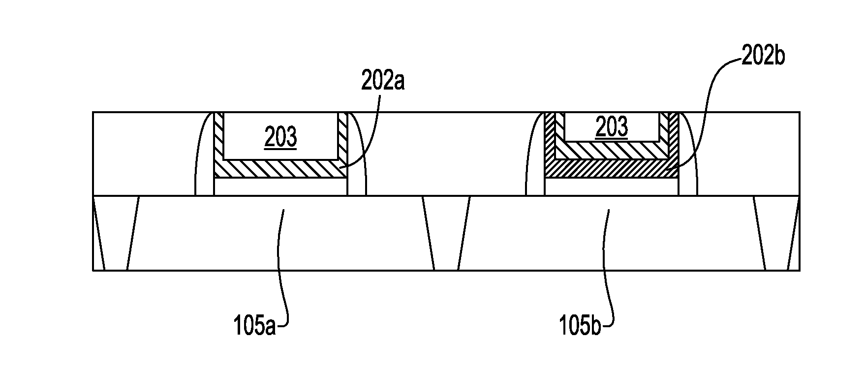
[0031]The present disclosure relates to forming a pFET device by controlling its work function (WF) employing a thick metal nitride alloy or carbon metal nitride alloy, both of which are nitrogen rich (1−X atoms of metal for X atoms of nitrogen, wherein X>0.5, e.g., two or more nitrogen atoms for each metal atom), and forming a complementary nFET device by controlling its WF employing the same metal nitride alloy or carbon metal nitride alloy, but having a thin layer of the aforementioned metal nitride alloy and which is metal-rich (1−X atoms of metal for X atoms of nitrogen where X<0.5, e.g., two or more metal atoms for each nitrogen atom).

[0032]The pFET and nFET transistors thus constructed and method of fabrication will now be described in greater detail by referring to the following description and drawings that accompany the present application. It is noted that the drawings of the present application are provided for illustrative purposes and, as such, they are not drawn to sc...


PUM


Abstract

A CMOS structure is formed on a semiconductor substrate that includes first and second regions having an nFET and a pFET respectively formed thereon. Each nFET and pFET device is provided with a gate, a source and drain, and a channel formed on the substrate. A high permittivity dielectric layer formed on top of the channel is superimposed to the permittivity dielectric layer. The pFET gate includes a thick metal nitride alloy layer or rich metal nitride alloy or carbon metal nitride layer that provides a controlled WF. Superimposed to the permittivity dielectric layer, the nFET gate is provided with a thin metal nitride alloy layer, enabling to control the WF. A metal deposition is formed on top of the respective nitride layers. The gate last approach characterized by having a high thermal budget smaller than 500° C. used for post metal deposition, following the dopant activation anneal.

Description

FIELD OF THE INVENTION[0001]The present invention relates to semiconductor devices and methods of fabricating, and more particularly, to a method for achieving a band-edge effective work function using the same metal through a CMOS gate. The present invention is applicable to planar or 3D devices by varying the thickness and nitrogen concentration of the eWF metal.BACKGROUND AND RELATED ART[0002]A “work function” (WF) is generally described as the energy, usually measured in electron volts, needed to remove an electron from the Fermi level to a point immediately outside the solid surface or the energy needed to move an electron from the Fermi level into vacuum. Work function is a material property of any material, whether the material is a conductor, semiconductor, or dielectric. For a metal, the Fermi level lies within the conduction band, indicating that the band is partly filled. For an insulator, the Fermi level lies within the band gap, indicating an empty conduction band; in t...

Claims


Application Information

Patent Timeline
IPC IPC(8): H01L27/092H01L21/8238
CPCH01L21/28088H01L29/4966H01L21/823857H01L21/823842H01L29/66545
Inventor ORTOLLAND, CLAUDEKWON, UNOHMURALI, KOTA V.R.M.NOWAK, EDWARD J.PANDEY, RAJAN KUMAR
Owner GLOBALFOUNDRIES INC
Why Eureka
Try Eureka