
Process for producing an organic semiconductor layer consisting of a mixture of a first and a second semiconductor

a technology of organic semiconductors and mixtures, which is applied in the field of manufacturing organic semiconductor layers, can solve the problems of difficult to accurately set the pore geometry, unstable solution, and inability to obtain such homogeneity with current deposition techniques, and achieve the effect of increasing accuracy and high density of pores

Active Publication Date: 2013-04-18
COMMISSARIAT A LENERGIE ATOMIQUE ET AUX ENERGIES ALTERNATIVES
View PDF6 Cites 0 Cited by
  • Summary
  • Abstract
  • Description
  • Claims
  • Application Information

AI Technical Summary

Benefits of technology

The present invention provides a method for manufacturing an organic semiconductor layer with two organic semiconductor materials that have a large contact surface area between them. This results in a porous volume made of the first semiconductor material having its pores at least partially impregnated with the second semiconductor material. This method allows for improved setting of the pore geometry and the removal of residues that could adversely affect the quality of the organic semiconductor layer. Additionally, this method results in a high-quality semiconductor layer with improved bonding between the two semiconductor materials and leads to a significant increase in the efficiency of organic photodiodes. The use of a gas allows for very fine porosity and a high density of pores distributed across the entire volume of the first material forming the porous volume. Furthermore, the gas bubbles can be adjusted in size to achieve increased accuracy in pore size.

Problems solved by technology

It is however not possible to obtain such a homogeneity with current deposition techniques.
As illustrated in FIGS. 2A-2D, this issue also arises when selecting a highly-volatile solvent, such as for example toluene.
Thus, when the two semiconductor materials are mixed in toluene to form a mixture which is initially as homogeneous as possible, for example, by magnetic stirring (FIG. 2A), the obtained solution is very unstable.
First, with such a porous volume manufacturing method, it is difficult to accurately set the pore geometry, and especially their dimensions, and there further remain residues of the second material, which adversely affects the quality of the organic semiconductor layer.

Method used


Image

  • Process for producing an organic semiconductor layer consisting of a mixture of a first and a second semiconductor
  • Process for producing an organic semiconductor layer consisting of a mixture of a first and a second semiconductor
  • Process for producing an organic semiconductor layer consisting of a mixture of a first and a second semiconductor

Examples


Embodiment Construction

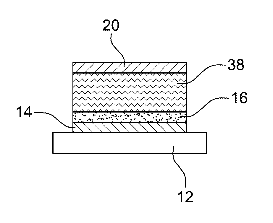
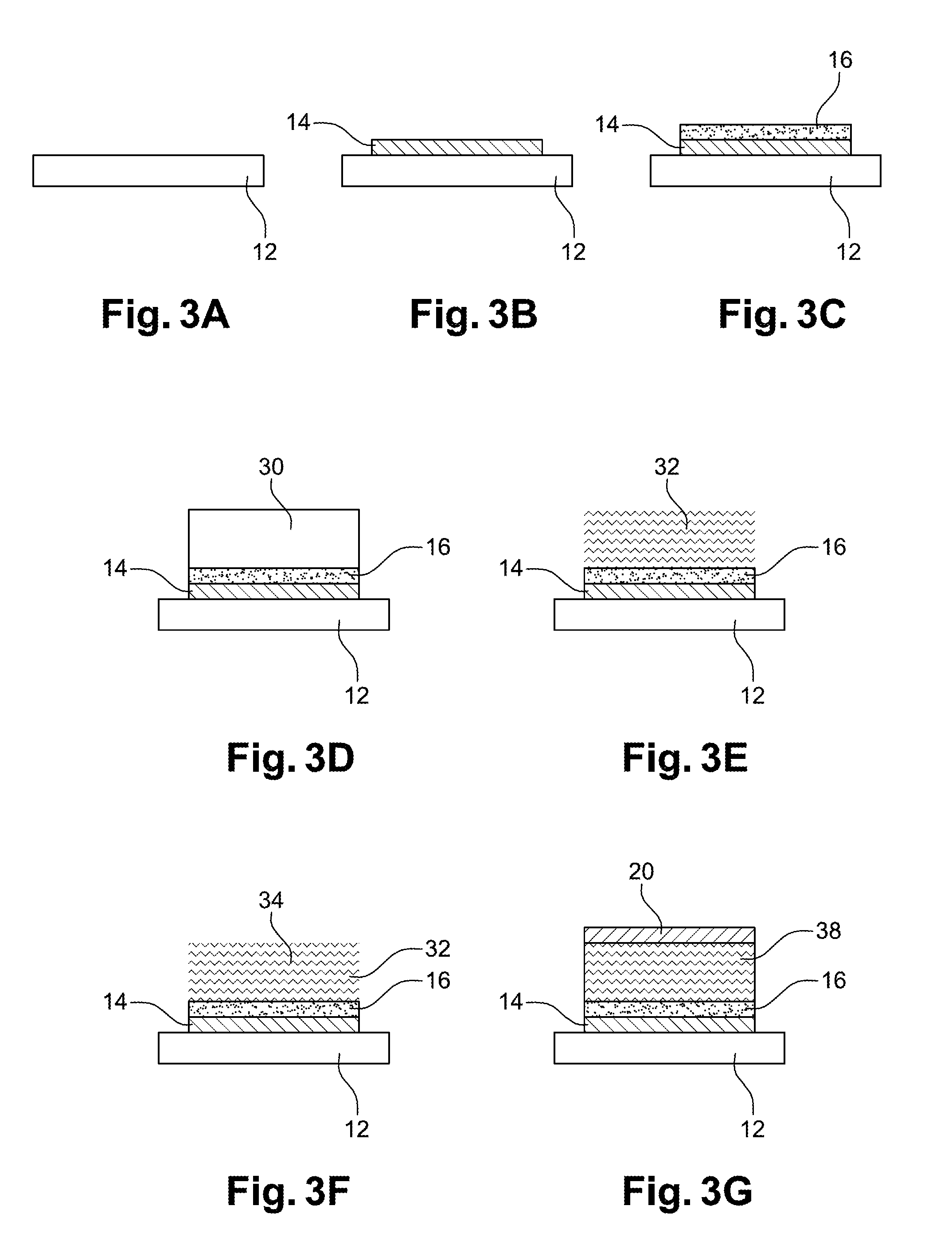
[0032]Referring to FIGS. 3A to 3G, a method for manufacturing an organic photodiode according to the invention conventionally starts with the forming of a glass substrate 12 (FIG. 3A), followed by the forming of an ITO metallization 14 by etching on substrate 12 to form the first electrode of the photodiode (FIG. 3B). The method then conventionally carries on with the deposition of a PEDOT:PPS injection layer 16 on first electrode 14 (FIG. 3C).

[0033]The method carries on with the manufacturing of a porous P3HT layer. More specifically, P3HT is dissolved or dispersed in a first solvent “B”, such as an alkane, for example. The solution thus obtained is mixed with a second solvent “C” non-miscible with first solvent “B”, having an evaporation temperature lower than that of first solvent “B”. For example, the first solvent is chlorobenzene or chloroform. The mixture thus obtained is emulsified, for example, by mechanical stirring, and emulsion 30 is deposited on injection layer 16 (FIG....


PUM

PropertyMeasurementUnit
widthaaaaaaaaaa
widthaaaaaaaaaa
organic semiconductoraaaaaaaaaa

Abstract

A method for manufacturing an organic semiconductor layer formed of a mixture of a first and of a second organic semiconductor materials includes the steps of: forming a porous solid volume formed of the first semiconductor material, of intercommunicating porosity and capable of receiving a second semiconductor material; depositing, at least on an external surface of the porous solid volume, a liquid including the second semiconductor material dissolved or dispersed in a solvent, the solvent being inert with respect to the first semiconductor material and having an evaporation temperature lower than the evaporation temperature of the second semiconductor material; and once the porous solid volume has been at least partially impregnated with the liquid, evaporating the solvent by heating up to a temperature higher than the evaporation temperature of said solvent and lower than the evaporation temperature of the first and of the second semiconductor materials.

Description

FIELD OF THE INVENTION[0001]The invention relates to the manufacturing of organic semiconductor layers formed of a mixture of a first and of a second semiconductor materials, more specifically of organic semiconductor layers taking part in the forming of organic optoelectronic devices, especially of photodiodes.BACKGROUND[0002]Referring to FIG. 1, which is a simplified cross-section view of a prior art organic photodiode 10, such a photodiode usually comprises a stack formed, from bottom to top:[0003]a transparent substrate 12, for example formed of a glass;[0004]a layer 14 forming a first electrode, for example, formed of an indium-tin oxide, usually called “ITO”;[0005]an injection layer 16, for example formed of a mixture of poly(3,4-ethylenedioxythiophene), commonly referred to as “PEDOT”, and of sodium poly(styrenesulfonate), commonly referred to as “PSS”, such a mixture being itself usually referred to as “PEDOT:PSS”. Injection layer 16 eases the passing of holes from first ele...

Claims


Application Information

Patent Timeline
Patent Type & Authority Applications(United States)
IPC IPC(8): H01L51/00H10K99/00
CPCH01L51/0003H01L51/0036H01L21/32056H01L51/0007H01L51/4253Y02E10/549H10K71/15H10K71/12H10K85/113H10K30/50H10K30/30
Inventor BENWADIH, MOHAMMED
Owner COMMISSARIAT A LENERGIE ATOMIQUE ET AUX ENERGIES ALTERNATIVES
Learn More