Organic el display panel, and method for producing same
- Summary
- Abstract
- Description
- Claims
- Application Information
AI Technical Summary
Benefits of technology
Problems solved by technology
Method used
Image

Examples
embodiment 1
Structure of Organic EL Display Panel 100
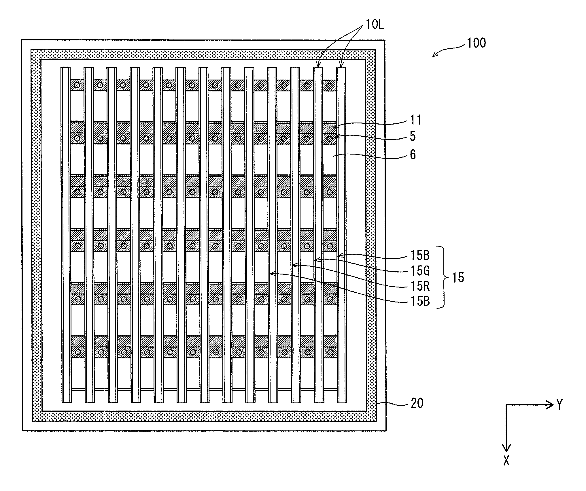
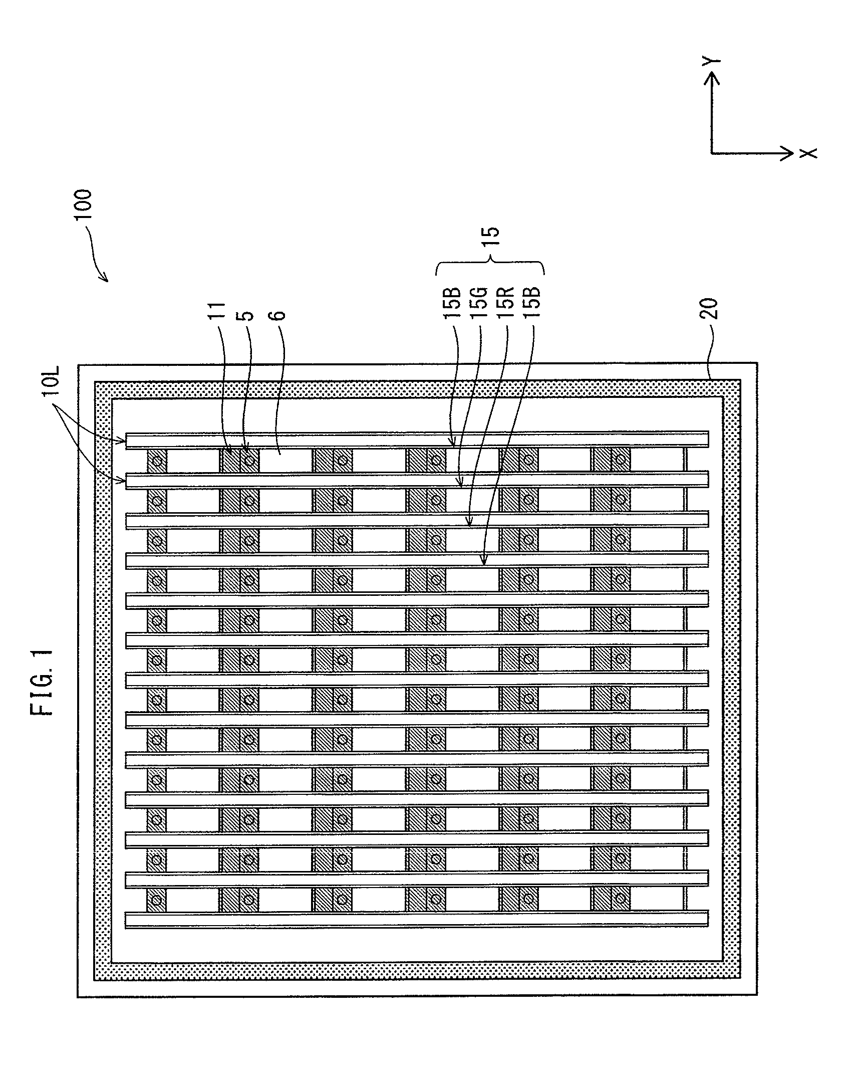
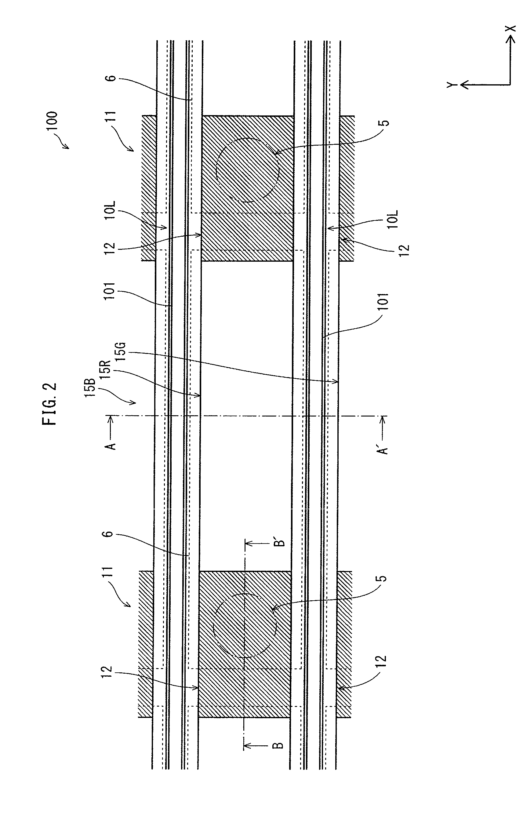
[0077]FIG. 1 is a top view showing the structure of a top-emission type organic EL display panel 100 (hereinafter, referred to just as “panel 100”) relating to Embodiment 1. FIG. 2 is a partial enlarged view showing the periphery of one organic EL element arranged on the panel 100. For convenience of explanation, the structure of a second electrode (cathode), a passivation layer, and so on arranged above an organic light-emitting layer 8 are omitted in FIG. 1 and FIG. 2. In FIG. 2, dashed lines indicate the shape of a first electrode 6, and two-dot chain lines indicate the shape of a contact hole 5.
[0078]According to the panel 100 as shown in FIG. 1, respective element formation regions are arranged in the column direction (X direction) and the row direction (Y direction). Organic EL elements 15 (specifically, 15R, 15G, and 15B) are arranged in a matrix in one-to-one correspondence with the element formation regions. In the row direction (Y d...
embodiment 2
[0140]FIG. 5 is a partial cross-sectional view showing a panel 100A relating to Embodiment 2, and corresponds to FIG. 3 showing the panel 100. The panel 100A has characteristics that a charge injection transport layer 7 is formed by an organic material such as PEDOT (polyethylenedioxythiophene) as an applying-type charge injection transport layer. In other words, in the step of forming functional layer, the charge injection transport layer 7 of the panel 100A is formed by applying an ink to the surface of the first electrode 6 between each two adjacent banks 10L and drying the applied ink. With this structure, the buried part 102 of the bank 10L is provided so as to directly contact each of the side surfaces of each of the adjacent first electrodes 6 and the inner surface of the opening 41 of the planarizing film 4.
[0141]According to the panel 100A having the above structure, it is possible to prevent color mixture of inks, thereby excellently forming an organic light-emitting layer...
embodiment 3
[0142]FIG. 6A is a top view schematically showing the structure of a panel 100B relating to Embodiment 3. In FIG. 6A, the recess degree of the bank 10L is adjusted such that a peripheral region of the panel 100B indicated by the sign “B” is higher in recess degree of the bank 10L than a central region of the panel 100B indicated by the sign “A”.
[0143]In the case where an ink is applied to an application target substrate, there is a problem of lateral distribution that color mixture of inks is likely to occur more often in the peripheral region B than the central region A. This is because of the following reason for example. When the application target substrate is moved or conveyed after the ink is applied to the panel, the angle relative to the horizontal direction is comparatively likely to vary in the peripheral region B. As a result, overflow of the ink in the peripheral region B is likely to be induced.
[0144]The panel 100B is formed in consideration of this problem. As shown in...
PUM
 Abstract
Description
Claims
Application Information
 - Generate Ideas
- Intellectual Property
- Life Sciences
- Materials
- Tech Scout
- Unparalleled Data Quality
- Higher Quality Content
- 60% Fewer Hallucinations
Browse by: Latest US Patents, China's latest patents, Technical Efficacy Thesaurus, Application Domain, Technology Topic, Popular Technical Reports.
© 2025 PatSnap. All rights reserved.Legal|Privacy policy|Modern Slavery Act Transparency Statement|Sitemap|About US| Contact US: help@patsnap.com