Magnetic nano-multilayers for magnetic sensors and manufacturing method thereof

a magnetic sensor and nano-multilayer technology, applied in nanoinformatics, instruments, record information storage, etc., can solve the problems of inconvenient manufacturing of devices, and inability to meet magnetic field sensitivity in both materials,

Active Publication Date: 2013-04-25
INST OF PHYSICS - CHINESE ACAD OF SCI
View PDF11 Cites 28 Cited by
  • Summary
  • Abstract
  • Description
  • Claims
  • Application Information

AI Technical Summary

Benefits of technology

[0019]As an improvement, the invention discloses the magnetic sensor as previously described, wherein, when external magnetic field is zero: the direction of the magnetic moment of the magnetic reference layer is parallel to that of the magnetic field under detection; and the direction of the magnetic moment of the magnetic detecting layer is perpendicular to that of the magnetic field under detection.
[0020]As an improvement, the invention discloses the magnetic sensor as previously described, wherein the pinning structure is an indirect pinning structure, said indirect pinning structure comprising one of: an antiferromagnetic layer (AFM)/a nonmagnetic metallic layer (NM)/a ferromagnetic layer (FM); and an antiferromagnetic layer (AFM)/a first nonmagnetic metallic layer (NM1)/a first ferromagnetic layer (FM1)/a second nonmagnetic metallic layer (NM2)/a second ferromagnetic layer (FM2).
[0021]As an improvement, the invention discloses the magnetic sensor as

Problems solved by technology

Both materials suffer from an inadequacy of sensitivity to magnetic fields.
Unfortunately, to embed a permanent magnetic film in the GMR spin value structure and in th

Method used


Image

  • Magnetic nano-multilayers for magnetic sensors and manufacturing method thereof
  • Magnetic nano-multilayers for magnetic sensors and manufacturing method thereof
  • Magnetic nano-multilayers for magnetic sensors and manufacturing method thereof

Examples


examples [UNK]

Examples 21˜26

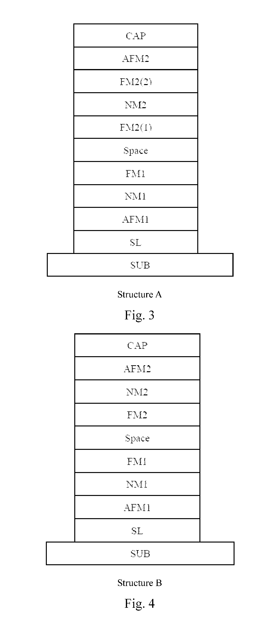
[0071]FIG. 7 shows the examples 21 through 26 applying the structure E: SUB / SL / AFM1 / FM1 / Space / FM2 / NM / AFM2 / CAP. Example 21 illustrates the method in which the magnetic nano-multilayers of structure E are made. The steps include:

[0072]1) Providing a substrate (SUB), the Si—SiO2 with a thickness of 1 mm. Also, depositing a seed layer Ta (5 nm) / Ru (20 nm) / Ta (5 nm) on the substrate with a magnetron sputtering deposition device under the following conditions: a vacuum better than 2×10⁻⁶ Pa, a deposition rate of 0.1 nm / s and an argon gas pressure of 0.07 Pa during deposition.

[0073]2) Depositing on the seed layer (SL) a layer of IrMn with the thickness of 15 nm, which is the first antiferromagnetic layer (AFM1), under the following conditions: a vacuum better than 2×10⁻⁶ Pa, a deposition rate of 0.1 nm / s and an argon gas pressure of 0.07 Pa.

[0074]3) Depositing on the AFM1 a layer of CoFeB with the thickness of 2.5 nm, this is the first ferromagnetic layer (FM1), under the fol...


PUM


Abstract

The invention discloses a magnetic nano-multilayers structure and the method for making it. The multilayer film includes—sequentially from one end to the other end—a substrate, a bottom layer, a magnetic reference layer, a space layer, a magnetic detecting layer and a cap layer. The, up-stated structure is for convert the information of the rotation of the magnetic moment of the magnetic detecting layer into electrical signals. The magnetic detecting layer is of a pinning structure to react to the magnetic field under detection. On the other hand, the invention sandwiches an intervening layer between the AFM and the FM to mitigate the pinning effect from the exchange bias. Moreover, the thickness of the intervening layer is adjustable to control the pinning effect from the exchange bias. The controllability ensures that the magnetic moments of the magnetic reference layer and the magnetic detecting layer remain at right angles to each other when the external field is zero. The invention achieves a GMR or TMR magnetic sensor exhibiting a linear response and by tuning the thickness of the non-magnetic metallic layer, the sensitivity as well as the detecting range of the devices can be tuned easily.

Description

BACKGROUND OF THE INVENTION[0001]The present invention generally relates to spintronics materials and magnetic sensors. More specifically, the invention relates to magnetic nano-multilayers for magnetic sensors and the manufacturing method thereof.[0002]The magnetic sensors are extensively applied in several areas such as the data storage, mechanical positioning, speed measuring and non-destructive detection.[0003]The magnetic sensors are primarily made of semiconductor materials exhibiting the Hall effect and the magnetic materials possessing anisotropic magnetoresistance (AMR). Both materials suffer from an inadequacy of sensitivity to magnetic fields. As the spintronics developed since 1988, the magnetic sensors built upon giant magnetorsistance [GMR] effect and tunnel magnetoresistance [TMR] have gained wider attention. Magnetic sensors based on spintronics materials have become popular for two reasons. One reason is that they are more sensitive. The other reason is that the tec...

Claims


Application Information

Patent Timeline
IPC IPC(8): G01R33/02
CPCB82Y25/00G01R33/093G11B5/3906H01L43/08G11C11/16B82Y10/00Y10S977/70G01R33/098G11B5/3909G11C11/161G11B2005/3996G01R33/02H10N50/10H01L2221/00H01L2223/00H01L21/00
Inventor MA, QINLILIU, HOUFANGHAN, XIUFENG
Owner INST OF PHYSICS - CHINESE ACAD OF SCI
Why Eureka
Try Eureka