Structure of field effect transistor with fin structure and fabricating method thereof

Active Publication Date: 2013-05-02
UNITED MICROELECTRONICS CORP
View PDF2 Cites 34 Cited by
  • Summary
  • Abstract
  • Description
  • Claims
  • Application Information

AI Technical Summary

Benefits of technology

[0007]To address these and other objectives, the present invention provides a method for fabricating a field effect transistor with fin structure. A substrate having an ion well with a first conductivity type is provided, wherein the ion well has a first doping concentration. At least a fin structure disposed on the substrate is formed. At least a first ion implantation is performed to form an anti-punch doped region with first conductivity type between the substrate and the channel layer, wherein the anti-punch doped region has a third doping concentration higher than the first doping concentration. At least a channel layer disposed along at least one surface of the fin structure is formed after the first ion implantation is performed. A gate covering part of the fin structure is formed. A source and a drain disposed in the fin structure beside the gate are formed, wherein the source and the drain h

Problems solved by technology

In a case that the top surface of the fin structure is covered by a patterned mask layer, however, exposed sidewal

Method used


Image

  • Structure of field effect transistor with fin structure and fabricating method thereof
  • Structure of field effect transistor with fin structure and fabricating method thereof
  • Structure of field effect transistor with fin structure and fabricating method thereof

Examples


first exemplary embodiment

The First Exemplary Embodiment

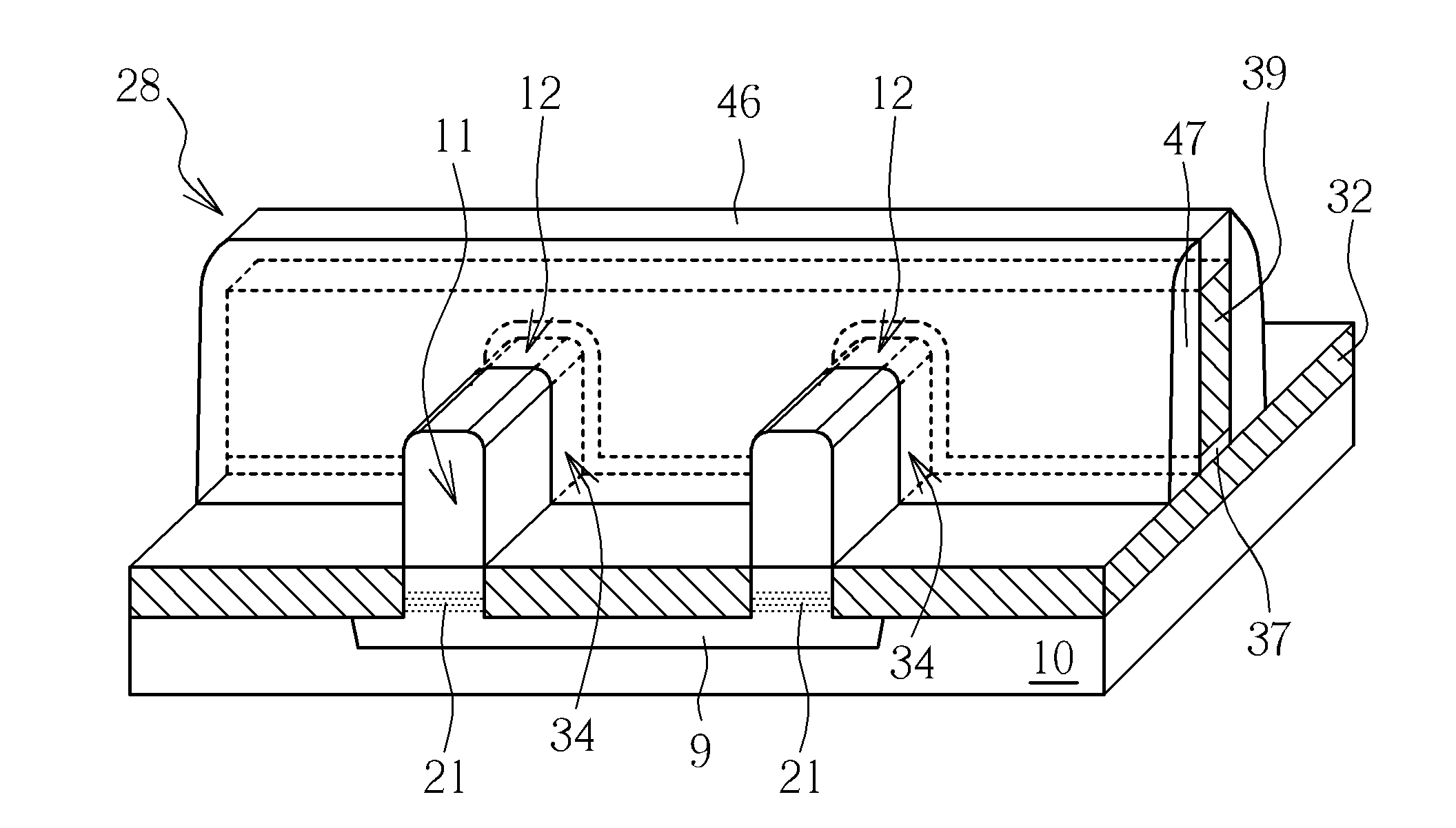
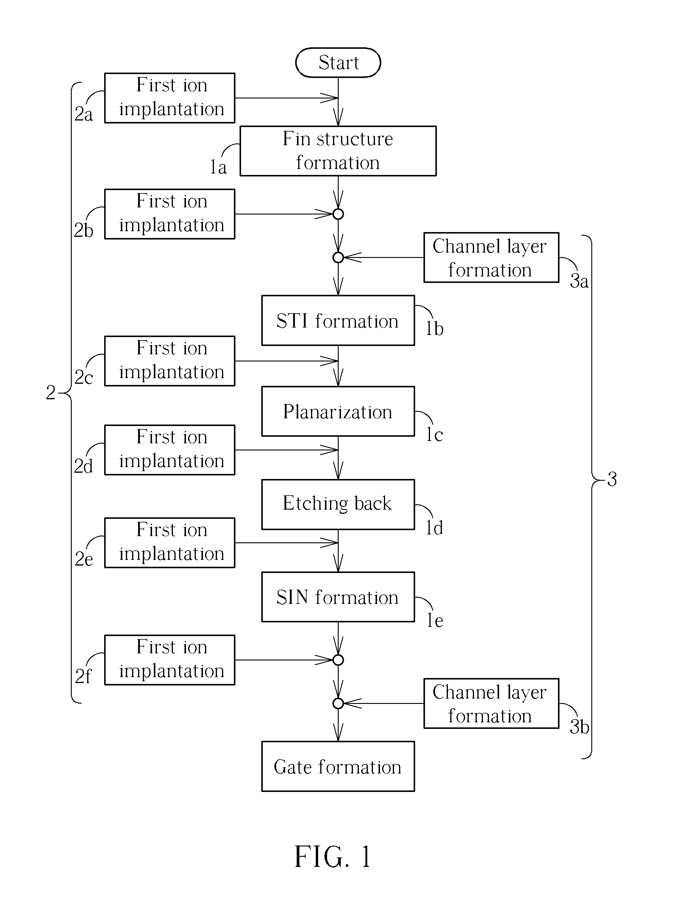
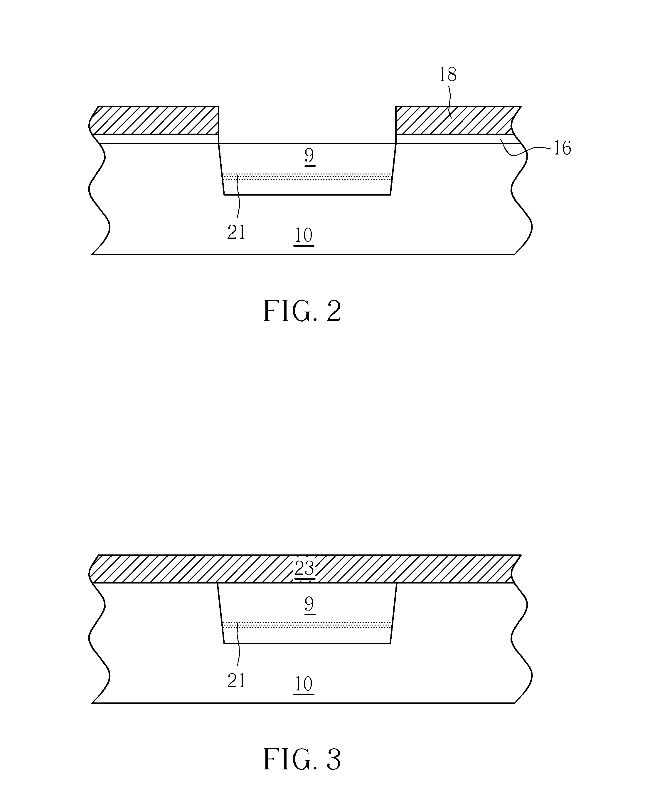
[0017]As illustrated in FIGS. 1-8, FIGS. 2-8 are schematic, cross-sectional view diagrams showing a method for fabricating a field effect transistor with fin structure according to the invention. In the first exemplary embodiment, the moment of performing the first ion implantation 2 is earlier than that of the fin structure forming 1a. As shown in FIG. 2, a substrate 10 covered with a patterned photoresist layer 18 is provided, wherein the patterned photoresist layer 18 is used to define the positions of an anti-punch doped region 21 and an ion well 9, that is to say, the anti-punch doped region 21 and the ion well 9 may be formed by using the same photomask. However, according to another embodiment, the ion well 9 and the anti-punch doped region 21 are fabricated by utilizing different photomasks. Next, an ion well 9 with a first conductivity type, e.g. P-type, is formed inside the substrate 10, wherein the ion well 9 has a first doping concentration,...

second exemplary embodiment

The Second Exemplary Embodiment

[0025]Please refer to FIG. 1 and FIGS. 3-8. The second exemplary embodiment is similar to the first exemplary embodiment and the main difference between them is that, in the second exemplary embodiment, the time of performing the first ion implantation 2 is at the time interval between fin structure formation 1a and STI formation 1b. Similar to FIG. 3, a substrate 10 covered with a semiconductor layer 23 is optionally provided and there is no anti-punch doped region in the substrate 10. Next, similar to FIG. 4, a second patterned mask layer 29 is formed on the semiconductor layer 23 to define the position of fin structure 11. By performing an etching process, at least a fin structure 11 is formed on the substrate 10 and is separated by a shallow trench 13. An etching process is performed to form at least a fin structure 11 on the substrate 10 while each fin structure 11 is separated by a shallow trench 13. Next, a first ion implantation 2 is carried ou...

third exemplary embodiment

The Third Exemplary Embodiment

[0026]Please refer to FIG. 1 and FIGS. 3-8. The third exemplary embodiment is similar to the second exemplary embodiment and the main difference between them is that, in the third exemplary embodiment, the time of performing the first ion implantation 2 is at the time interval between STI formation 1b and the planarization 1c process. Similar to FIG. 3, a substrate 10 covered with a semiconductor layer 23 is provided and there is no anti-punch doped region in the substrate 10. Next, similar to FIGS. 3-4, at least a fin structure 11 is formed on the substrate 10 and is separated by a shallow trench 13. An etching process is performed to form at least a fin structure 11 on the substrate 10 while each fin structure 11 is separated by a shallow trench 13. Subsequently, as illustrated in FIG. 5, through a high density plasma CVD (HPCVD) process, a sub atmosphere CVD (SACVD) process or a spin on dielectric (SOD) process, an insulation layer 31 covering the fi...


PUM


Abstract

A method for fabricating a field effect transistor with fin structure includes the following steps. A substrate having an ion well with a first conductivity type is provided, wherein the ion well has a first doping concentration. At least a fin structure disposed on the substrate is formed. At least a first ion implantation is performed to form an anti-punch doped region with first conductivity type between the substrate and the channel layer, wherein the anti-punch doped region has a third doping concentration higher than the first doping concentration. At least a channel layer disposed along at least one surface of the fin structure is formed after the first ion implantation is performed. A gate covering part of the fin structure is formed. A source and a drain disposed in the fin structure beside the gate are formed, wherein the source and the drain have a second conductivity type.

Description

BACKGROUND OF THE INVENTION[0001]1. Field of the Invention[0002]The present invention generally relates to the field of field effect transistors (FETs) with fin structure. More particularly, the present invention relates to the structure of a field effect transistor with fin structure and fabricating method thereof.[0003]2. Description of the Prior Art[0004]With the trend in the industry being towards scaling down the size of metal oxide semiconductor transistors (MOS), three-dimensional or non-planar transistor technology, such as fin field effect transistor technology (Fin FET) has been developed to replace planar MOS transistors. The three-dimensional structure of a fin FET increases the overlapping area between the gate and the fin structure of the silicon substrate, and accordingly, the channel region is more effectively controlled. The drain-induced barrier lowering (DIBL) effect and short channel effect is therefore reduced. The channel region is also longer under the same ga...

Claims


Application Information

Patent Timeline
IPC IPC(8): H01L29/772H01L21/336
CPCH01L29/7851H01L29/66795
Inventor LIN, CHIEN-TING
Owner UNITED MICROELECTRONICS CORP
Why Eureka
Try Eureka