Packaging substrate having embedded capacitors and fabrication method thereof

a technology of capacitors and packaging substrates, which is applied in the direction of printed circuit manufacturing, printed circuit aspects, stacking capacitors, etc., can solve the problems of limited functions of packaging substrates, inability to meet multi-function requirements, and increase so as to increase the combinational and selective functions of capacitors and reduce the height of the overall structure

Active Publication Date: 2013-05-02
UNIMICRON TECH CORP
View PDF3 Cites 23 Cited by
  • Summary
  • Abstract
  • Description
  • Claims
  • Application Information

AI Technical Summary

Benefits of technology

[0016]Therefore, by stacking the first and second capacitors in the cavity through the bonding layer, the single core layer is embedded with two stacked capacitors so as to increase combinational and selective functions of the capacitors, thereby meeting the multi-function requirement.
[0017]Furthermore, by eliminating the need to stack another packaging substrate having an embedded capacitor as required in the prior art, the present invention reduces the height of the overall structure to thereby meet the miniaturization or thinning requirement.

Problems solved by technology

Therefore, such a packaging substrate has limited functions and accordingly cannot meet the multi-function requirement.
On the other hand, in order to meet the multi-function requirement, several packaging substrates can be stacked on one another, which, however, leads to an increase in height of the overall structure.
As such, the structure cannot meet the miniaturization or thinning requirement.

Method used


Image

  • Packaging substrate having embedded capacitors and fabrication method thereof
  • Packaging substrate having embedded capacitors and fabrication method thereof
  • Packaging substrate having embedded capacitors and fabrication method thereof

Examples


Embodiment Construction

[0020]The following illustrative embodiments are provided to illustrate the disclosure of the present invention, these and other advantages and effects can be apparent to those in the art after reading this specification.

[0021]It should be noted that all the drawings are not intended to limit the present invention. Various modification and variations can be made without departing from the spirit of the present invention. Further, terms such as “one”, “on”, “top”, “bottom” etc. are merely for illustrative purpose and should not be construed to limit the scope of the present invention.

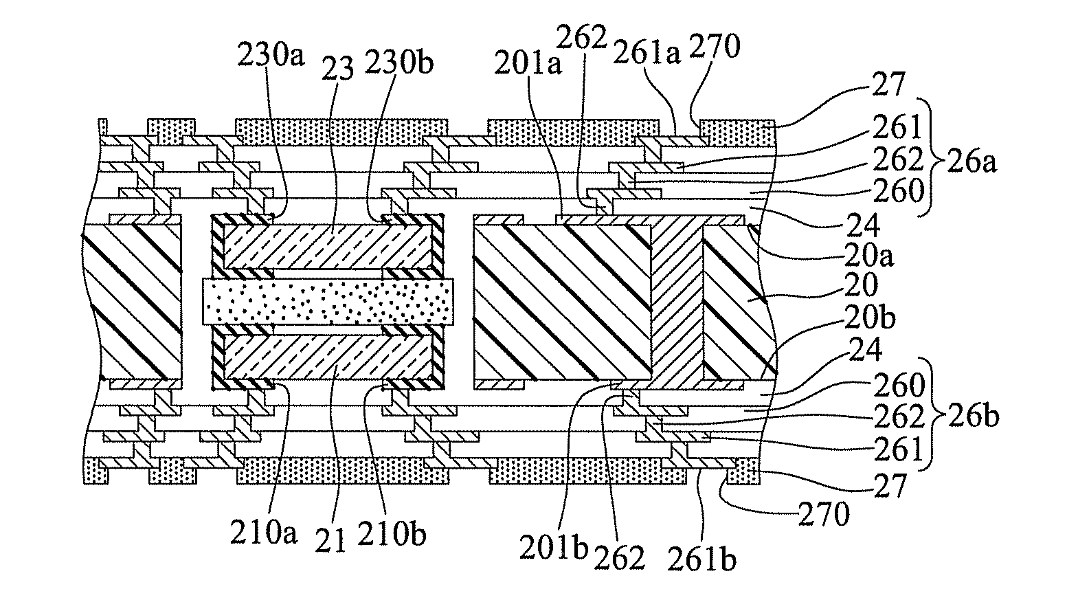
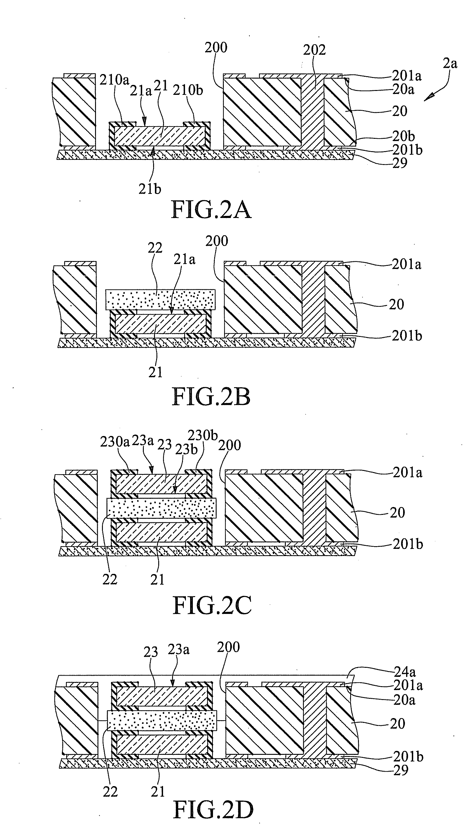
[0022]FIGS. 2A to 2G are schematic cross-sectional views showing a fabrication method of a packaging substrate 2 having embedded capacitors according to the present invention.

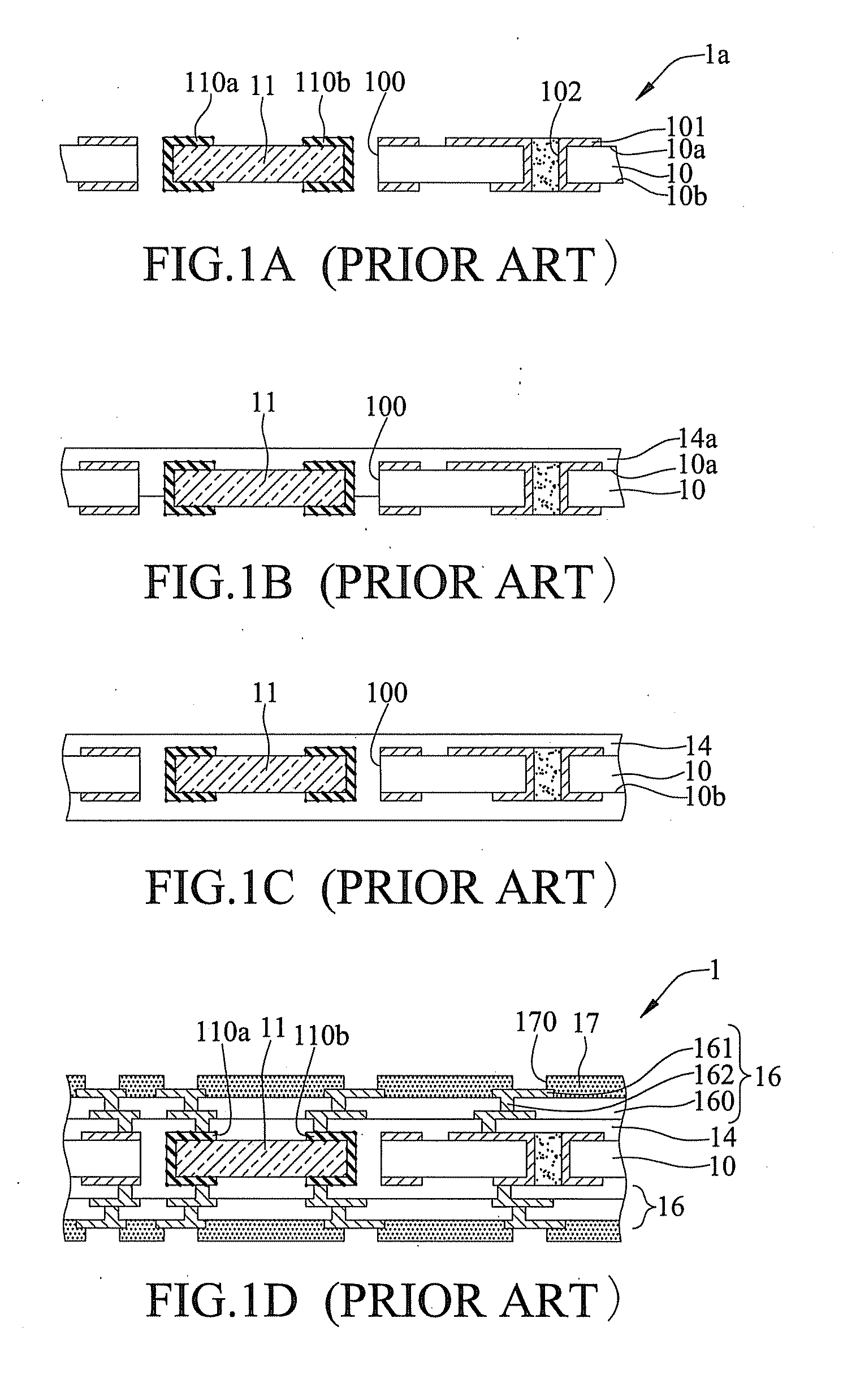
[0023]Referring to FIG. 2A, a substrate 2a is provided. The substrate 2a has a core layer 20 having opposite first and second surfaces 20a, 20b, a cavity 200 in communication with the first and second surfaces 20a, 20b of the core l...


PUM

PropertyMeasurementUnit
dielectricaaaaaaaaaa
insulatingaaaaaaaaaa
adhesiveaaaaaaaaaa

Abstract

A packaging substrate includes: a substrate having a core layer, a cavity penetrating the core layer and circuit layers formed on surfaces of the core layer; a first capacitor disposed in the cavity; a bonding layer formed on the first capacitor in the cavity of the substrate; a second capacitor disposed on the bonding layer so as to be received in the cavity; and a dielectric layer formed on the substrate and in the cavity for covering the first and second capacitors. By stacking the first and second capacitors in the cavity through the bonding layer, the single core layer is embedded with two layers of the capacitors to thereby meet the multi-function requirement.

Description

BACKGROUND OF THE INVENTION[0001]1. Field of the Invention[0002]The present invention relates to packaging substrates and fabrication methods thereof, and more particularly, to a packaging substrate having embedded capacitors and a fabrication method thereof.[0003]2. Description of Related Art[0004]Along with the rapid development of semiconductor packaging technologies, different package types have been developed for semiconductor devices. To reduce the height of packages so as to meet the miniaturization or thinning requirement of products, semiconductor components are generally embedded in cavities of packaging substrates so as to reduce the volume of the overall semiconductor devices and improve the electrical performance.[0005]FIGS. 1A to 1D are schematic cross-sectional views showing a fabrication method of a packaging substrate 1 having an embedded capacitor according to the prior art. Referring to FIG. 1A, a substrate 1a is provided, which has a core layer 10 having opposite...

Claims


Application Information

Patent Timeline
Patent Type & Authority Applications(United States)
IPC IPC(8): H01L27/08H01L21/50
CPCH01L23/498H01L23/49822H01L23/49827H01L21/48H01L23/64H01L28/40H01G4/30H01L2924/0002H05K3/4602H05K2201/10515H05K1/185H05K2201/10015H01L2924/00H01L23/642
Inventor LAI, CHIEN-KUANGHUANG, CHUN-CHIH
Owner UNIMICRON TECH CORP
Why Eureka
Try Eureka