Semiconductor device, power converter and method for controlling the power converter

Active Publication Date: 2013-05-02
PANASONIC CORP
View PDF0 Cites 6 Cited by
  • Summary
  • Abstract
  • Description
  • Claims
  • Application Information

AI Technical Summary

Benefits of technology

[0018]In a semiconductor device according to an embodiment of the present invention, in a power converter that uses SiC-MISFETs where both forward current and reverse current are made to flow through the same ch

Problems solved by technology

And that reverse recovery current causes not only recovery loss but also a decrease in switching rate as well.
However

Method used


Image

  • Semiconductor device, power converter and method for controlling the power converter
  • Semiconductor device, power converter and method for controlling the power converter
  • Semiconductor device, power converter and method for controlling the power converter

Examples


embodiment 1

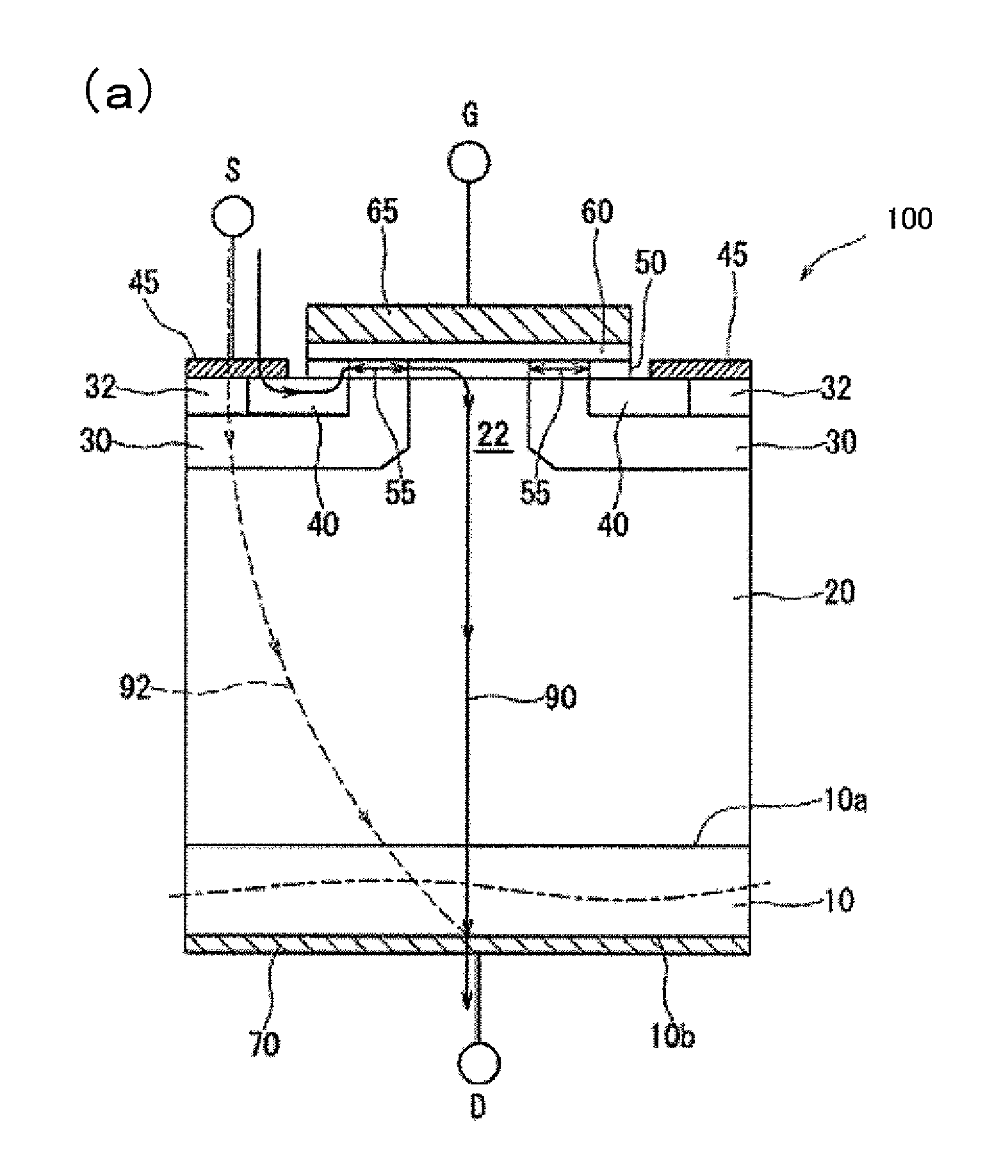
[0080]Hereinafter, a first embodiment of a semiconductor device, power converter and its control method according to the present invention will be described. Any pair of components shown in multiple drawings to be referred to in the following description but having substantially the same function will be identified herein by the same reference numeral for the sake of simplicity.

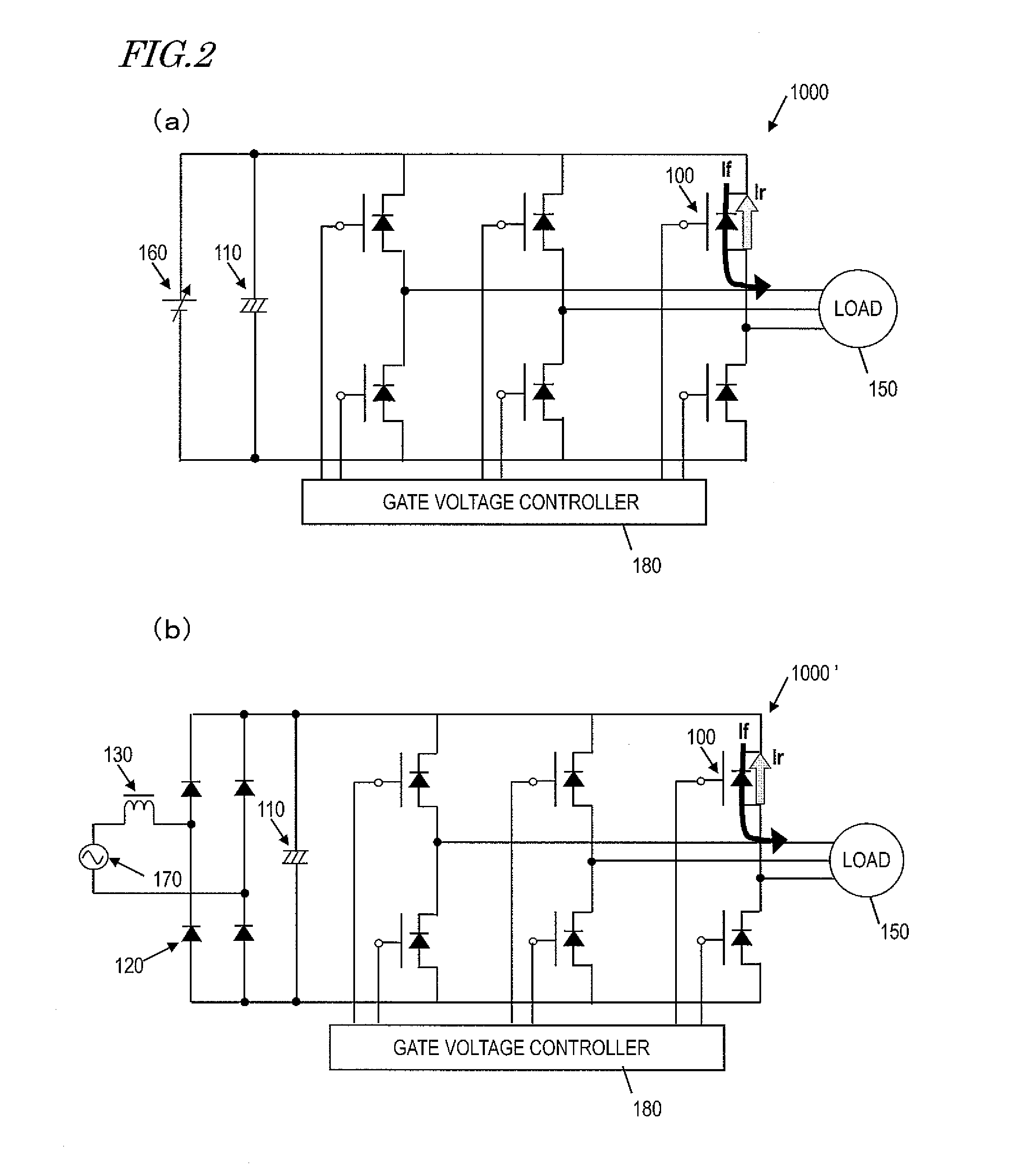
[0081]Portion (a) of FIG. 6A illustrates a configuration for a power converter 2000 as a first embodiment of the present invention. Just like the circuit shown in FIG. 2, the power converter 2000 is a circuit for driving an inductive load 150 such as a motor, converts a DC power supply 160 into an AC power and supplies that power to the load 150. The power converter 2000 typically includes an inverter circuit comprised of multiple semiconductor elements 100 and a gate voltage controller 180. Although the power converter 2000 usually does not include any DC power supply 160, the DC power supply 160 is also sho...

embodiment 2

[0139]Hereinafter, a second embodiment of a semiconductor element according to the present invention will be described.

[0140]As already described for the first embodiment, each of the SiC-MISFETs 200a and 200b may have a normal three-terminal package form (e.g., TO220) with gate, source and drain terminals as shown in FIG. 3. In that case, the respective active regions 13 of the SiC-MISFETs 200a and 200b are separately packaged on two different substrates.

[0141]Meanwhile, the SiC-MISFETs 200a and 200b of this embodiment are characterized by being arranged on the same substrate. FIG. 14 schematically illustrates a planar structure of a semiconductor element 201 as a second embodiment of the present invention. The semiconductor element 202 includes SiC-MISFETs 200a and 200b that are arranged on the same silicon carbide substrate 10. Each of the SiC-MISFETs 200a and 200b has a number of unit structures, each having the structure shown in FIG. 1(a). The SiC-MISFETs 200a and 200b may be ...

embodiment 3

[0146]FIG. 15 schematically illustrates the planar structure of a semiconductor element 202 as a third embodiment of the present invention. The semiconductor element 202 also includes SiC-MISFETs 200a and 200b that are arranged on the same silicon carbide substrate 10 but has a girdling region 12 that is provided in common to surround both of the active regions 13a and 13b, which is a difference from the second embodiment described above.

[0147]As shown in FIG. 15, the SiC-MISFETs 200a and 200b may be arranged in active regions 13a and 13b, respectively.

[0148]In this semiconductor element 202, a gate electrode pad 14a is arranged on the silicon carbide substrate 10. The gate electrode pad 14a is connected to the gate electrode of the SiC-MISFET 200a in the active region 13a and to a gate line (not shown). Likewise, another gate electrode pad 14b is arranged on the silicon carbide substrate 10 and is connected to the gate electrode of the SiC-MISFET 200b in the active region 13b and t...


PUM


Abstract

Disclosed is a semiconductor device which includes: a semiconductor element 200 including a first metal-insulator-semiconductor field-effect transistor 200a and a second metal-insulator-semiconductor field-effect transistor 200b which is connected in parallel with the first metal-insulator-semiconductor field-effect transistor; and a control section which controls the operation of the semiconductor element. The control section controls the semiconductor element so that in a forward direction mode, current flows in a forward direction through the first and second metal-insulator-semiconductor field-effect transistors but that in a reverse direction mode, current flows in the reverse direction through the first metal-insulator-semiconductor field-effect transistor but does not flow through the second metal-insulator-semiconductor field-effect transistor.

Description

TECHNICAL FIELD[0001]The present invention relates to a semiconductor device and more particularly relates to a silicon carbide semiconductor device (as a power semiconductor device) which can be used in applications that require a high breakdown voltage and a large amount of current. The present invention also relates to a power converter including a silicon carbide semiconductor device and a method for controlling such a power converter.BACKGROUND ART[0002]Recently, there is a growing demand for a power converter (inverter) that can drive a load operating with alternating current such as a motor as efficiently as possible with its overall size and cost reduced as much as possible. To meet such a demand, a field effect transistor made of silicon carbide has been developed as a switching element for a power converter.[0003]Silicon carbide (SiC) is a high-hardness semiconductor material with a greater bandgap than silicon (Si), and has been used extensively in various kinds of semico...

Claims


Application Information

Patent Timeline
IPC IPC(8): H03K17/06H02M7/537H01L29/78
CPCH01L29/78H03K17/164H03K17/063H02M7/003H01L23/4824H01L29/7828H01L29/7838H01L29/0619H01L29/0696H01L29/1608H01L2924/0002H02M7/537H03K17/12H01L2924/00
Inventor HAYASHI, MASASHIOGAWA, MASANORI
Owner PANASONIC CORP
Why Eureka
Try Eureka