Wiring structure, thin film transistor array substrate including the same, and display device

a technology of thin film transistors and array substrates, applied in semiconductor devices, semiconductor/solid-state device details, instruments, etc., can solve the problems of reducing the yield reducing the reliability of tft array substrates, so as to achieve excellent electrical connection and suppress the occurrence of film floating

Active Publication Date: 2013-05-09
TRIVALE TECH
View PDF0 Cites 7 Cited by
  • Summary
  • Abstract
  • Description
  • Claims
  • Application Information

AI Technical Summary

Benefits of technology

[0011]An object of the present invention is to provide a wiring structure capable of suppressing occurrence of film floating of an insulating film on a transparent conductive film, and obtaining excellent electrical connection between the transparent conductive film and a metal film, a TFT array substrate including the same, and a liquid crystal display device.
[0013]Concentration of stress on an end of the first transparent conductive film is prevented, and occurrence of film floating of an insulating film provided on the first transparent conductive film can be suppressed. Further, since the first transparent conductive film is connected to the end surface, exposed inside the hollow portion, of the first conductive film, excellent electrical connection can be obtained by other layer even when the electrical connection between an uppermost layer of the first conductive film and the first transparent conductive film is poor.

Problems solved by technology

Since a function of the insulating film as a protective film is lost on the portion where the film floating of the insulating film occurs, the film floating leads to reduction in corrosion resistance of an electrode, occurrence of dielectric breakdown, or the like, which causes reduction in a yield on the manufacture of the TFT array substrate and reduction in reliability of the TFT array substrate.
For example, since excellent electrical connection cannot be easily obtained between a transparent electrode such as ITO (Indium Tin Oxide) and Al, a problem arises when an ITO transparent conductive film is required to be disposed on a laminated film having an Al-based metal as an uppermost layer.

Method used


Image

  • Wiring structure, thin film transistor array substrate including the same, and display device
  • Wiring structure, thin film transistor array substrate including the same, and display device
  • Wiring structure, thin film transistor array substrate including the same, and display device

Examples


first preferred embodiment

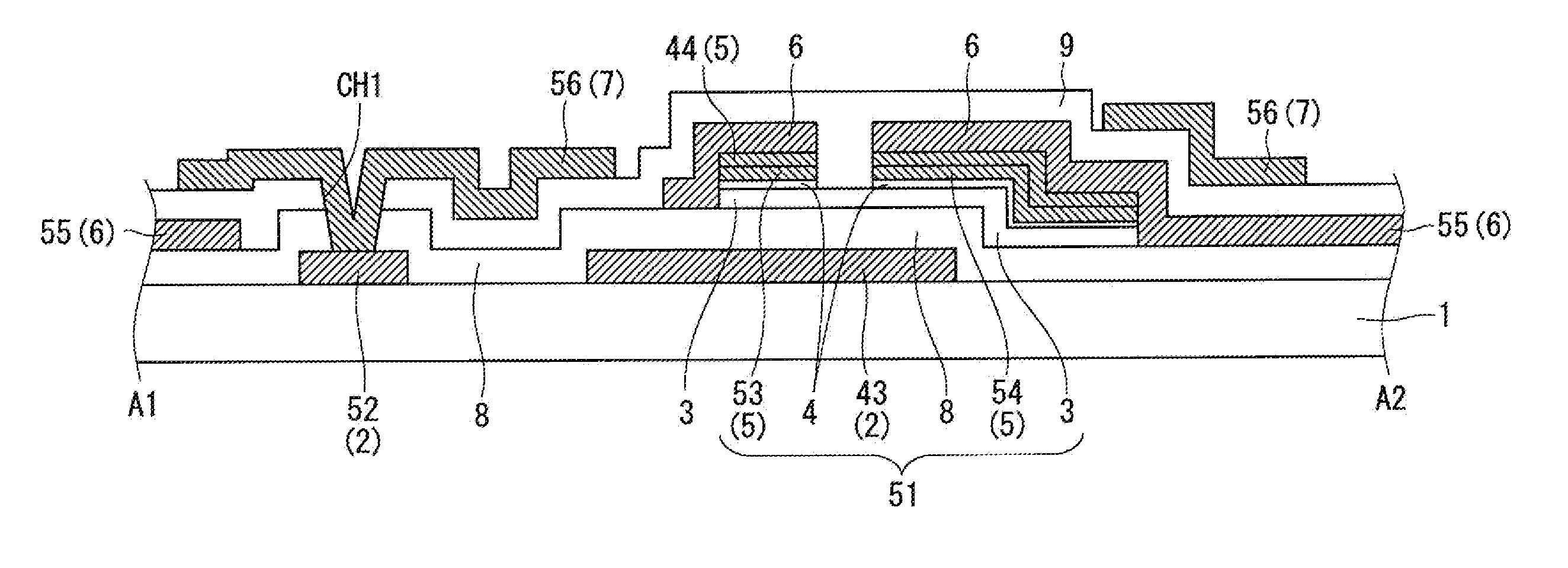
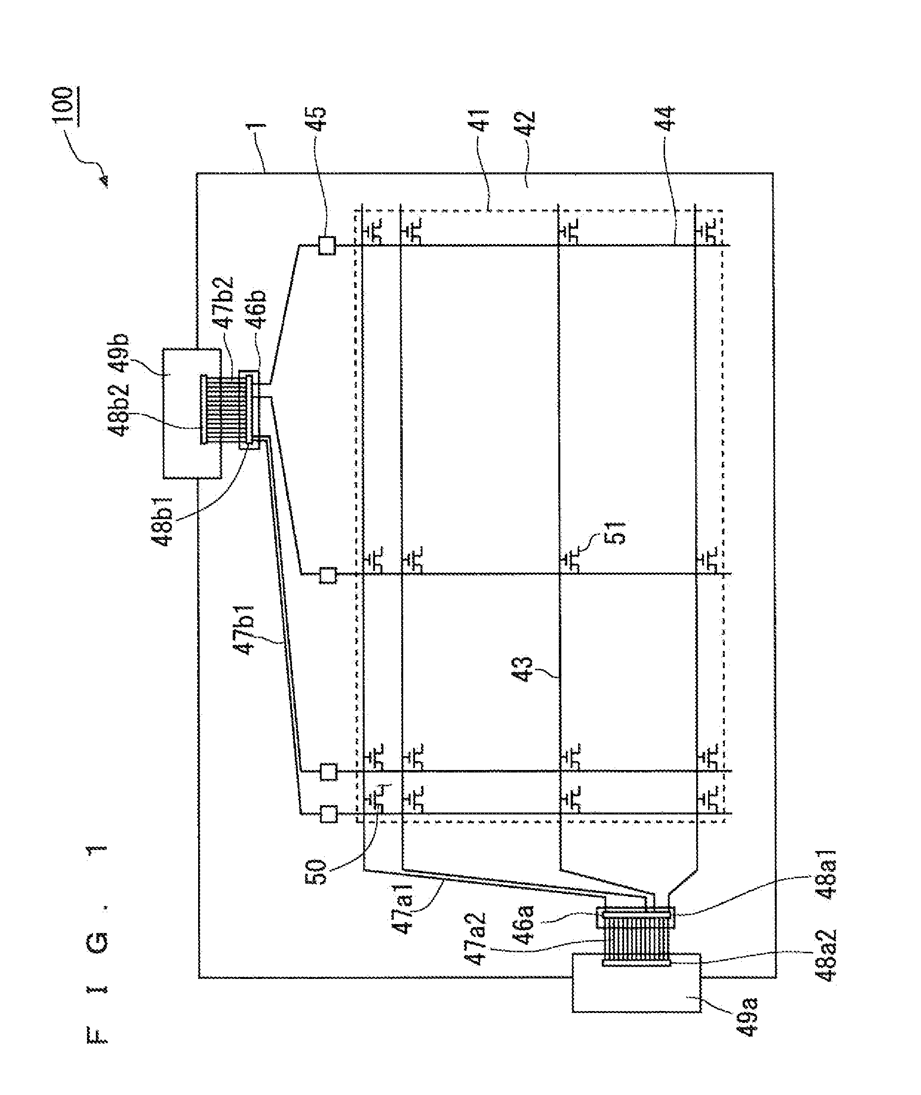
[0036]First, a configuration example of a liquid crystal display device capable of applying a wiring structure according to the present invention is shown. FIG. 1 is a plan view showing a TFT array substrate 100 configuring the liquid crystal display device according to a preferred embodiment of the present invention. As shown in FIG. 1, the TFT array substrate 100 includes pixels 50 serving as units of display of an image, which are disposed on a substrate 1 in a form of an array (matrix). Each pixel 50 is provided with a TFT 51 serving as a switching element that supplies a display voltage to a pixel electrode (not shown). A member formed from the substrate 1 equipped with the TFTs 51 is called a “TFT array substrate” since the TFTs 51 are arranged for the respective pixels 50 in the form of an array. The substrate 1 is configured, for example, by a glass substrate or a semiconductor substrate.

[0037]The TFT array substrate 100 includes an array region 41 (region inside a rectangle...

second preferred embodiment

[0130]FIG. 16 and FIG. 17 are views showing a configuration of a wiring conversion part 45 of a TFT array substrate 100 according to a second preferred embodiment. FIG. 16 is a plan view of the wiring conversion part 45, and FIG. 17 is a sectional view taken along D1-D2 in FIG. 16.

[0131]The wiring conversion part 45 of the second preferred embodiment is configured such that, unlike the configuration of the first preferred embodiment (FIG. 5, FIG. 7), a hollow portion 13 exposing an end surface of a second conductive film 5 inside the second conductive film 5 and contact holes CH2 for connecting a second transparent conductive film 7 to a first transparent conductive film 6 are disposed on positions different from each other. In the example of FIG. 16, two contact holes CH2 are provided, and the hollow portion 13 is disposed between the two contact holes CH2. Additionally, two contact holes CH3 for connecting the second transparent conductive film 7 to a first conductive film 2 are a...

third preferred embodiment

[0134]FIG. 18 and FIG. 19 are views showing a configuration of a wiring conversion part 45 of a TFT array substrate 100 according to a third preferred embodiment. FIG. 18 is a plan view of the wiring conversion part 45, and FIG. 19 is a sectional view taken along E1-E2 in FIG. 18.

[0135]The wiring conversion part 45 of the third preferred embodiment is configured such that, unlike the configuration of the first preferred embodiment (FIG. 5, FIG. 7), a first transparent conductive film 6 is also provided with an opening corresponding to the hollow portion 13. That is, the first transparent conductive film 6 is not formed on an inner portion of the hollow portion 13, and formed only on an upper surface of a second conductive film 5.

[0136]A contact hole CH2 is formed so as to include the hollow portion 13 similarly to the first preferred embodiment. As a result, end surfaces of the second conductive film 5, an ohmic contact film 4, and the semiconductor film 3 exposed on the hollow port...


PUM


Abstract

On a wiring conversion part connected to a first conductive film and a second conductive film each functioning as a wiring, a hollow portion is formed inside the second conductive film. A first transparent conductive film provided on the second conductive film is formed so as to cover an upper surface of the second conductive film and an end surface thereof exposed on the hollow portion, and so as not to cover an outer peripheral end surface of the second conductive film. A second transparent conductive film which is a layer above the first transparent conductive film is connected to the second conductive film and the first conductive film, so that the first conductive film and the second conductive film are electrically connected.

Description

BACKGROUND OF THE INVENTION[0001]1. Field of the Invention[0002]The present invention relates to a wiring structure including a wiring of a transparent conductive film, which is disposed, for example, on a display panel of a liquid crystal display device or the like.[0003]2. Description of the Background Art[0004]Recently, as a liquid crystal mode capable of achieving both characteristics of a wide viewing angle and high transmittance, adoption of an FFS (Fringe Field Switching) mode to a liquid crystal display device has been rapidly spread. An FFS mode TFT array substrate includes a structure in which two layers of transparent conductive films are overlapped with an insulating film therebetween, as shown, for example, in Japanese Patent No. 3826217. On the other hand, a transparent conductive film included in a general TN (Twisted Nematic) mode TFT array substrate is a single layer. Accordingly, the number of photoengraving steps required for manufacturing the FFS mode TFT array s...

Claims


Application Information

Patent Timeline
Patent Type & Authority Applications(United States)
IPC IPC(8): H01L23/48
CPCH01L27/124H01L2924/0002G02F1/1345H01L2924/00
Inventor NAGANO, SHINGOSHIMAMURA, TAKESHIHOKA, NARUHITO
Owner TRIVALE TECH
Why Eureka
Try Eureka