Large area nitride crystal and method for making it

a nitride crystal, large-area technology, applied in the direction of polycrystalline material growth, crystal growth process, after-treatment details, etc., can solve the problems of high density, difficult to produce dislocation density, and high density of dislocation crystals, and achieve high quality

Active Publication Date: 2013-05-16
SLT TECH
View PDF3 Cites 101 Cited by
  • Summary
  • Abstract
  • Description
  • Claims
  • Application Information

AI Technical Summary

Problems solved by technology

The typical average dislocation density, however, in these crystals, about 106-108 cm−2, is too high for many applications.
Techniques have been developed to gather the dislocations into bundles or low-angle grain boundaries, but it is still very difficult to produce dislocation densities below 104 cm−2 in a large area single grain by these methods, and the relatively high concentration of high-dislocation-density bundles or grain boundaries creates difficulties such as performance degradation and / or yield losses for the device manufacturer.
Unfortunately, no large area, high quality non-polar or semi-polar GaN wafers are generally available for large scale commercial applications.
These crystals, however, are typically small, less than 1 −5 centimeters in diameter, and are not commercially available.
Such legacy techniques, however, have limitations.
For example, legacy techniques do not specify the accuracy of the crystallographic orientation between the merged elementary seed crystals they provide a method capable of producing highly accurate crystallographic registry between the elementary seed crystals and the observed defects resulting from the merging of the elementary seed crystals.
Conventional techniques are inadequate for at least the reason of failing to meaningfully increase the available size of high-quality nitride crystals while maintaining extremely accurate crystallographic orientation across the crystals.

Method used


Image

  • Large area nitride crystal and method for making it
  • Large area nitride crystal and method for making it
  • Large area nitride crystal and method for making it

Examples


example 1

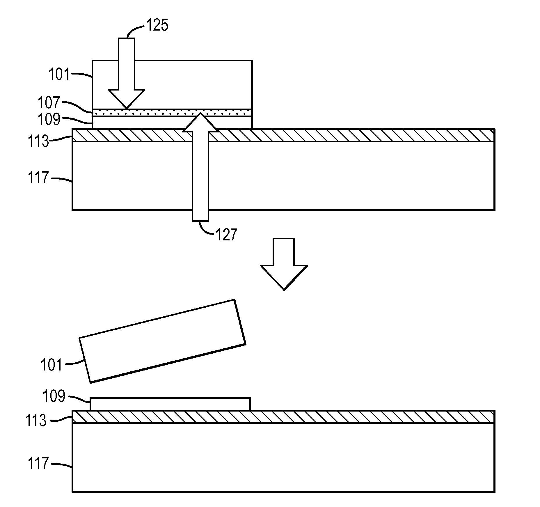
[0091]A template was prepared using four HVPE-grown bulk GaN crystals wafer-bonded to a handle substrate, also comprising HVPE-grown bulk GaN. The nitride crystals exhibited a crystallographic orientation within 1 degree of the (0 0 0 1) +c-plane (Ga face). The adjoining surfaces of the nitride crystals and the handle substrate were each coated with a 200 Angstrom Ti layer followed by a 1.5 micron Au layer and wafer-bonded at a pressure of 5.4 MPa and a temperature of 450° C. under vacuum. The gaps between adjacent bonded nitride crystals were approximately 85 microns. The misorientation angles α, β, and γ between the adjacent bonded nitride crystals were all less than 0.1 degrees. The template was degreased, suspended by a silver wire, and placed in a silver capsule with a baffle. Approximately 37.3 g of polycrystalline GaN, 1.27 g of NH4F mineralizer, and 30.4 g of ammonia were also placed in the capsule and the capsule was hermetically sealed. The capsule was placed in an interna...

example 2

[0092]A template was prepared using two HVPE-grown bulk GaN crystals bonded to a handle substrate, also comprising HVPE-grown bulk GaN. The nitride crystals exhibited a crystallographic orientation within 1 degree of the (0 0 0 1) +c-plane (Ga face). The adjoining surfaces of the handle substrate and the nitride crystals were coated with a 200 Angstrom Ti layer followed by a 1.0 micron Au layer. The nitride crystals further had an array of 300 micron diameter Si dots having a height of 0.6 microns, the dots being located at the vertices of a square grid having a period of 1,000 microns in both the x- and y-directions. The handle substrate was then placed on a heated stage at 475° C. and a pick and place tool was used to precisely position the two nitride crystals on the handle substrate. The adjoining surfaces of the nitride crystals and the handle substrate, while precisely aligned, were placed in contact for approximately 30 seconds and a bond was formed. The misorientation angles...

example 3

[0093]A template was prepared using three HVPE-grown bulk GaN crystals bonded to a handle substrate, also comprising HVPE-grown bulk GaN. The nitride crystals exhibited a crystallographic orientation that was miscut from the {1 0 −1 0} m-plane by approximately 0.25 degree toward [0 0 0 −1]. The adjoining surfaces of the handle substrate and the nitride crystals were coated with a 200 Angstrom Ti layer followed by approximately a 20 micron thick Au layer and 3 micron thick AuSn layer on the handle substrate and the nitride crystals, respectively. The handle substrate was then placed on a heated stage at 330° C. and a pick and place tool was used to precisely position the three nitride crystals on the handle substrate. The adjoining surfaces of the nitride crystals and the handle substrate, while precisely aligned, were placed in contact for approximately 30 seconds and a bond was formed. The template was degreased and placed in a silver capsule with a baffle. Approximately 4,815 g of...


PUM


Abstract

Techniques for processing materials in supercritical fluids including processing in a capsule disposed within a high-pressure apparatus enclosure are disclosed. The disclosed techniques are useful for growing crystals of GaN, AlN, InN, and their alloys, including InGaN, AlGaN, and AlInGaN for the manufacture of bulk or patterned substrates, which in turn can be used to make optoelectronic devices, lasers, light emitting diodes, solar cells, photoelectrochemical water splitting and hydrogen generation devices, photodetectors, integrated circuits, and transistors.

Description

CROSS REFERENCE TO RELATED APPLICATIONS[0001]This application is a continuation-in-part of, and claims priority to U.S. application Ser. No. 13 / 160,307, filed on Jun. 14, 2011, which claims priority to U.S. Provisional Application No. 61 / 356,489, filed on Jun. 18, 2010; and to U.S. Provisional Application No. 61 / 386,879, filed on Sep. 27, 2010; each of which is incorporated herein by reference for all purposes.BACKGROUND[0002]This disclosure relates to techniques for processing materials in supercritical fluids. Embodiments of the disclosure include techniques for material processing in a capsule disposed within a high-pressure apparatus enclosure. The methods can be applied to growing crystals of GaN, AlN, InN, and their alloys, including, for example, InGaN, AlGaN, and AlInGaN, and others for the manufacture of bulk or patterned substrates. Such bulk or patterned substrates can be used for a variety of applications including optoelectronic devices, lasers, light emitting diodes, s...

Claims


Application Information

Patent Timeline
Patent Type & Authority Applications(United States)
IPC IPC(8): H01L21/02H01L29/20
CPCH01L21/02609H01L29/2003C30B33/06C30B25/18C30B29/403C30B25/02C30B7/105C30B19/068C30B19/12C30B29/406H01L21/0254
Inventor D'EVELYN, MARK P.SPECK, JAMES S.KAMBER, DERRICK S.POCIUS, DOUGLAS W.
Owner SLT TECH
Why Eureka
Try Eureka