Making transparent capacitor with multi-layer grid

a capacitor and multi-layer technology, applied in capacitor manufacturing, conductive material removal by irradiation, instruments, etc., can solve the problems of limited power supply limited substrate materials, limited current carrying capacity of such electrodes, etc., to achieve simple layer alignment, increase conductivity and transparency, and avoid heating materials

Inactive Publication Date: 2013-05-30
EASTMAN KODAK CO
View PDF6 Cites 21 Cited by
  • Summary
  • Abstract
  • Description
  • Claims
  • Application Information

AI Technical Summary

Benefits of technology

[0015]The present invention provides an improved apparatus and method for providing increased conductivity and transparency to the electrodes of a capacitive device that is scalable to large sizes, avoids heating materials in sensitive locations, enables

Problems solved by technology

However, the current-carrying capacity of such electrodes is limited, thereby limiting the amount of power that can be supplied to the pixel elements.
Moreover, the substrate materials are limited by the deposition process (e.g. sputtering).
Thicker layers of metal oxides or metals increase conductivity but reduce the transparency of the electrodes.
However, the formation of such metal grids is problematic.
Sputtering through a shadow mask is difficult for large substrates due to thermal expansion and alignment problems of the shadow mask.
Likewise, evaporative deposition of conductive materials such as metals requires high temperatures and suffers from the same mask problems.
High temperatures can also destroy any temperature-sensitive underlying layers or substrates.
The use of photolithography to pattern metal layers, metal-oxide layers, or metal grids can compromise the integrity of underlying layers.
Furthermore, a metal grid is not transparent and can cover only a relat

Method used


Image

  • Making transparent capacitor with multi-layer grid
  • Making transparent capacitor with multi-layer grid
  • Making transparent capacitor with multi-layer grid

Examples


Embodiment Construction

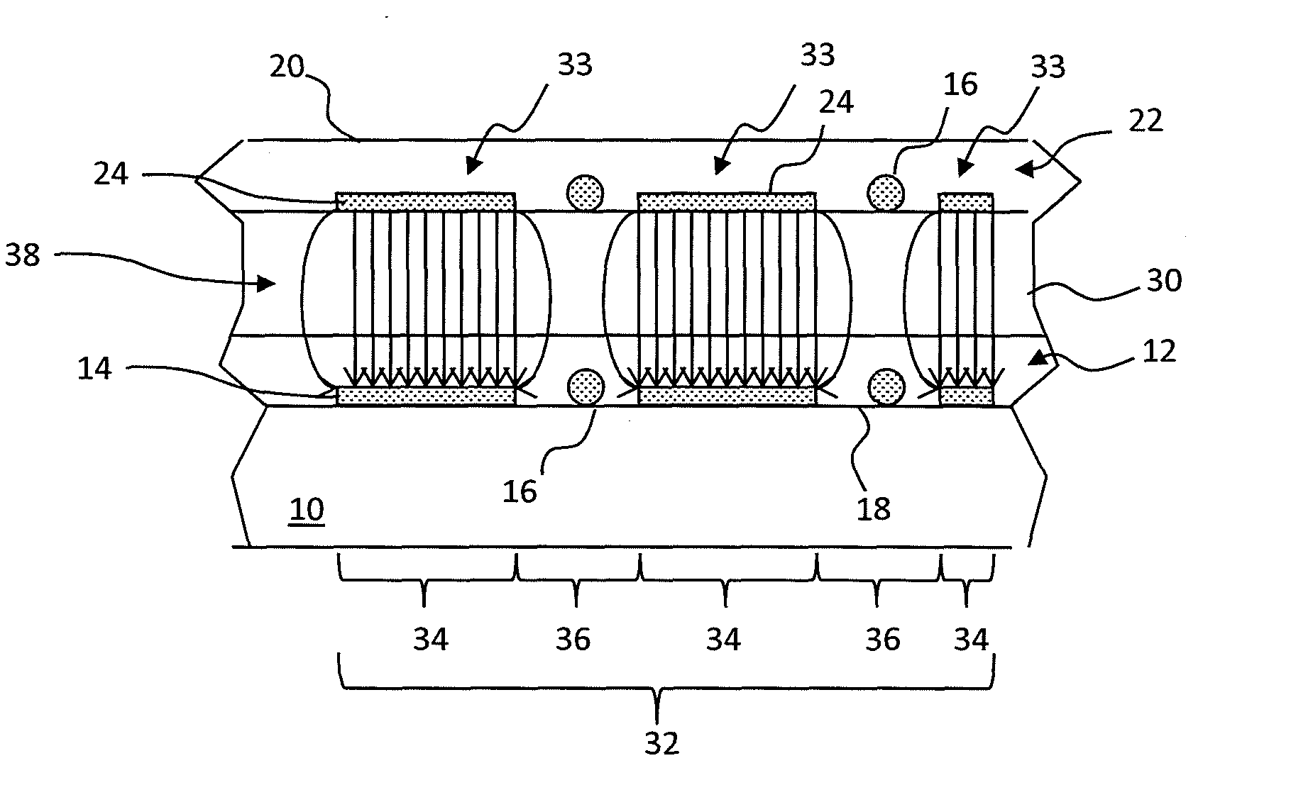
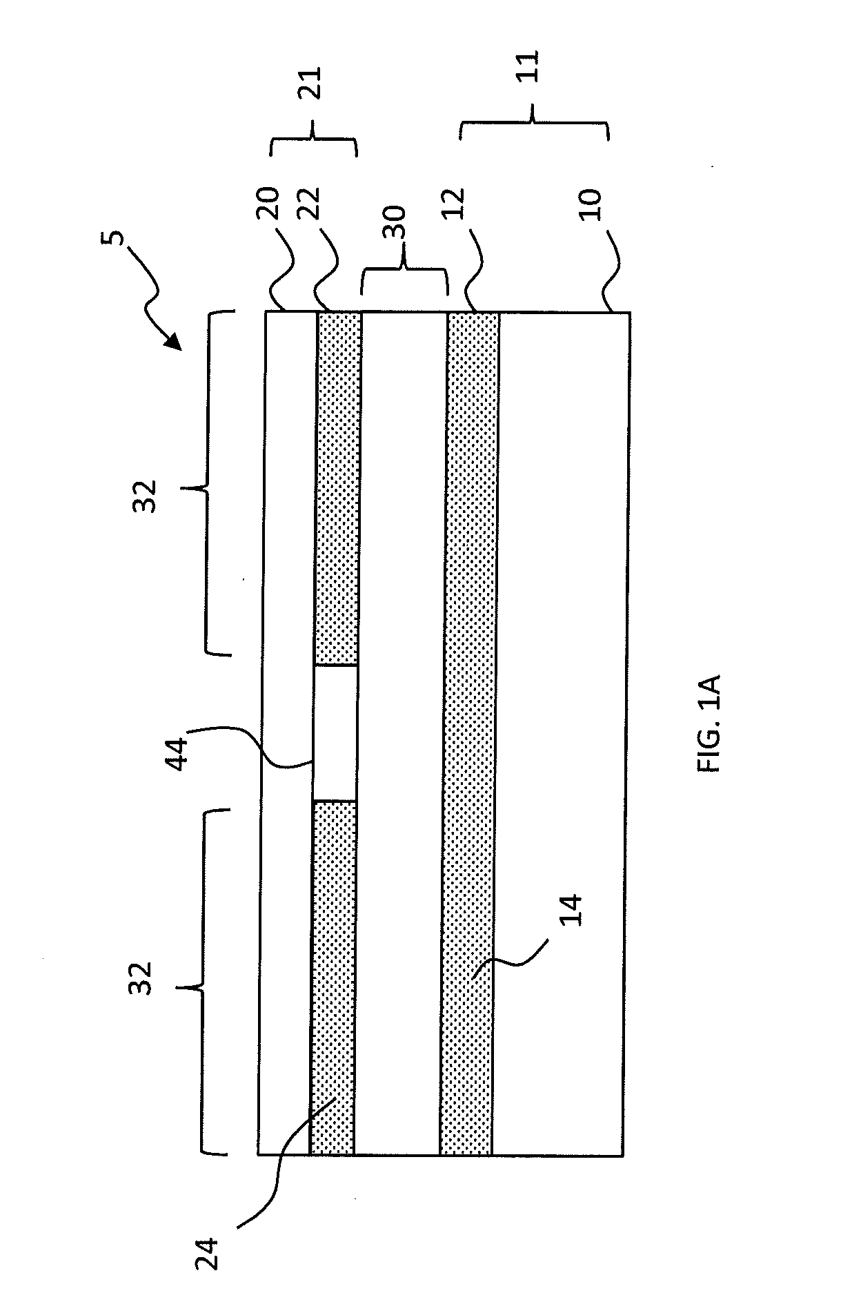
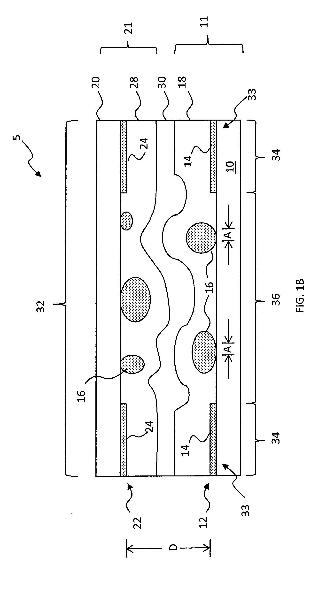
[0040]Referring to FIG. 1A according to an embodiment of the present invention, a transparent capacitor apparatus 5 includes a first transparent substrate 10 including a first patterned conductive layer 12 having a first conductive material 14 located over the first transparent substrate 10 forming a first substrate structure 11. A dielectric layer 30 is located over the first patterned conductive layer 12. A second patterned conductive layer 22 including a second conductive material 24 is located over the dielectric layer 30. The pattern of the second patterned conductive layer 22 is different from the pattern of the first patterned conductive layer 12. The first and second patterned conductive layers 12, 14 include gaps 44 defining the patterns. A second transparent substrate 20 is located over the dielectric layer 30, for example over the second patterned conductive layer 22 forming a second substrate structure 21. Portions 32 of the first conductive material 14 of the first patt...


PUM

PropertyMeasurementUnit
Dielectric polarization enthalpyaaaaaaaaaa
Electrical conductoraaaaaaaaaa
Surfaceaaaaaaaaaa

Abstract

A method of making a transparent capacitor apparatus includes: providing a first transparent substrate including a first patterned conductive layer having a first pattern; providing a second transparent substrate including a second patterned conductive layer having a second pattern different from the first pattern; locating the first transparent substrate over the second transparent substrate so that the first patterned conductive layer is effectively parallel to the second patterned conductive layer. Overlapping portions of both the first conductive layer and the second conductive layer are patterned time into spatially matching conductive areas and non-conductive areas by locally applying heat to melt conductive materials in the non-conductive areas so that the surface tension of the conductive materials causes the conductive materials to coalesce into structures with a reduced conductive layer area.

Description

CROSS-REFERENCE TO RELATED APPLICATIONS[0001]Reference is made to commonly-assigned, co-pending U.S. patent application Ser. No. ______ (Kodak Docket K000538US01) filed concurrently herewith, entitled “TRANSPARENT CAPACITOR WITH MULTI-LAYER GRID STRUCTURE” by MITCHELL BURBERRY, ET AL., the disclosure of which is incorporated herein.FIELD OF THE INVENTION[0002]The present invention relates to transparent capacitors.BACKGROUND OF THE INVENTION[0003]Transparent conductors are widely used in the flat-panel display industry to form electrodes that are used to electrically switch the light-emitting or light-transmitting properties of a display pixel, for example in liquid crystal or organic light-emitting diode displays. Transparent conductors are also used to create electrodes for transparent capacitors used in capacitive touch-screen in conjunction with displays. In such displays, the transparency and conductivity of the transparent electrodes are important attributes. In general, it is...

Claims


Application Information

Patent Timeline
IPC IPC(8): G01R27/26H01G13/00H01J9/00
CPCG06F3/044G06F2203/04111G06F2203/04103G02F1/13439G06F2203/04102H01G4/005H01G4/008H05K1/162H05K3/027H05K3/4626H05K3/4673H05K2203/107H05K2203/1194G06F3/0445G06F3/0446
Inventor BURBERRY, MITCHELL STEWARTCOK, RONALD STEVEN
Owner EASTMAN KODAK CO
Why Eureka
Try Eureka