Apparatus and method for measuring a luminescent decay

a technology of luminescent decay and measurement method, which is applied in the direction of luminescent dosimeters, optical radiation measurement, fluorescence/phosphorescence, etc., can solve the problems of absorbing electrical energy from cracks and defects, and wasting the whole purpose of solar cells

Active Publication Date: 2013-06-06
YSYST
View PDF0 Cites 12 Cited by
  • Summary
  • Abstract
  • Description
  • Claims
  • Application Information

AI Technical Summary

Benefits of technology

[0037]The present invention enables the measurement of information related to the carrier lifetime inside of a material, without physical contact, by monitoring the light emitted from that material.
[0038]Moreover, this invention makes it possible to measure the uniformity of the carrier lifetime over an area of the material.

Problems solved by technology

Such cracks and defects absorb the electrical energy that the cell has converted from optical energy.
In other words, the whole purpose of the solar cell, to generate electrical energy from light is wasted if the carriers of this energy encounter cracks which then converts this energy into heat.
Also these methods require the fabrication process to reach near completion before they can be performed.
It is difficult to implement such processes in mass production environments without slowing down the fabrication or causing scratches and affecting the cleanliness due to contact application.
In the single photon counting method, the emission decay trace is measured directly however the time required to obtain the histogram is too long to be practically applied to the full wafer area.
Whereas the streak camera method is forbiddingly costly.

Method used


Image

  • Apparatus and method for measuring a luminescent decay
  • Apparatus and method for measuring a luminescent decay
  • Apparatus and method for measuring a luminescent decay

Examples


Embodiment Construction

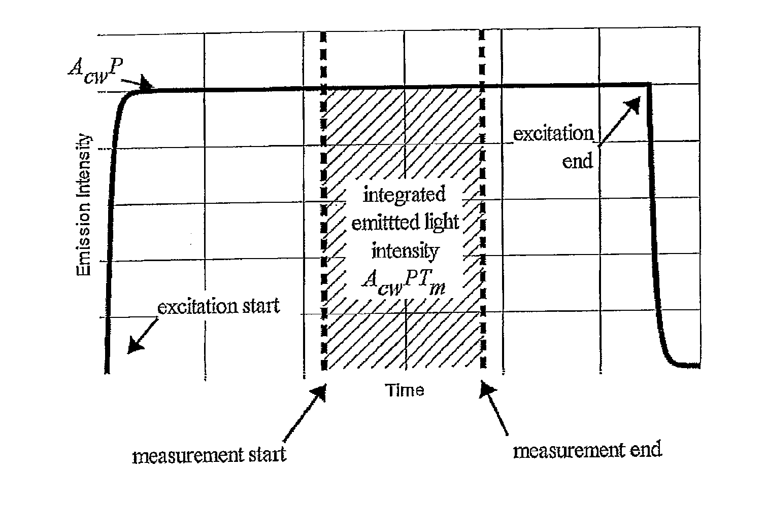
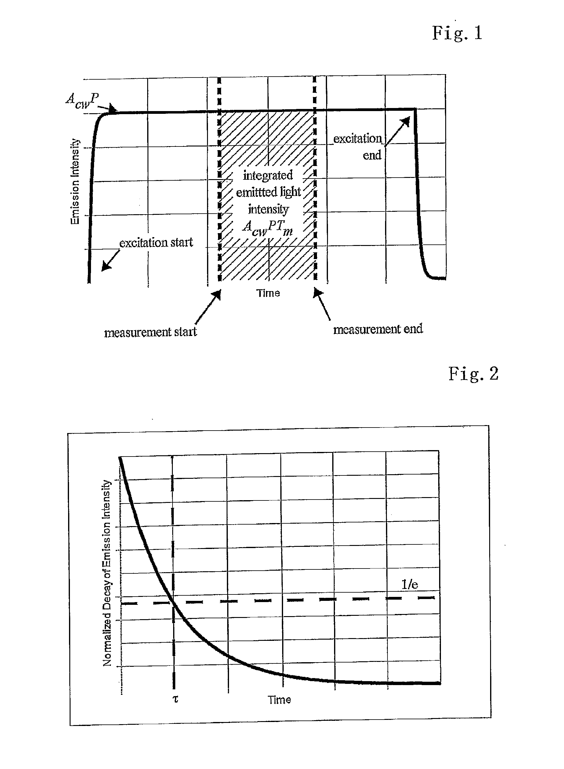
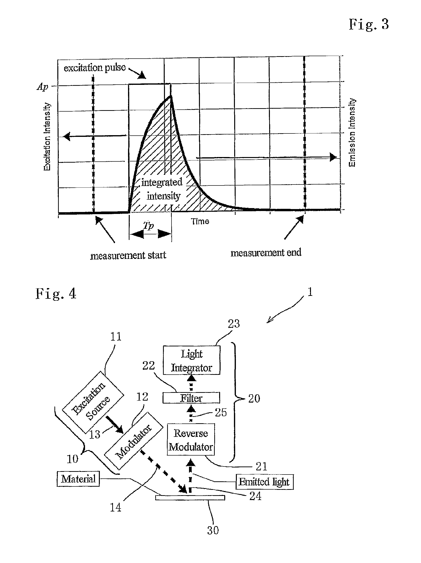
[0070]In order to evaluate a material such as a semiconductor, the current invention measures the light emitted (luminescence) from that material.

[0071]The energy of a non-valence electron in the crystal of a material is determined by the position of the conduction band, but can also be determined by a variety of states such as non-radiative centers, impurity levels, or other defect states. If an electron is in a non-thermal-equilibrium excited state, it will eventually recombine with a hole within a probable time giving rise to a carrier lifetime. That recombination causes an energy conversion which can be in the form of light emission, or in the form of vibrations or heat in the material. If the carrier recombines due to defects, impurities or cracks in the crystal, then the probability of emitting light due to natural recombination will be reduced. Because of this, in general the carrier lifetime is shorter in the presence of a high density of crystal defects. Therefore a measure...


PUM

PropertyMeasurementUnit
modulation frequencyaaaaaaaaaa
frequencyaaaaaaaaaa
frequencyaaaaaaaaaa

Abstract

[Problem] An apparatus and method for measuring luminescence decay due to the lifetime of energy carriers inside a material such as a semiconductor is presented.[Solution] The intensity of a laser is modulated by a light modulating device resulting in a square wave excitation 14, and applied to a semiconducting material. The energy carriers inside the semiconductor are excited, and recombine after a certain time to give rise in part to some light emission 24, which decays in intensity from the time at which the excitation periods end. The decaying light is separated from the light emitted during excitation by another light modulator resulting in 26. This light intensity 26 contains the information related to the carrier lifetime. Because the amount of this light 26 is small and has a very short emission time, a CCD detector is used to be integrated several cycles of the decay periods in order to obtain a reasonable signal. This integrated intensity signal can be used to determine the carrier lifetime.

Description

TECHNICAL FIELD[0001]This invention relates to a measurement method and to an apparatus for measuring the carrier lifetime of a material, by first exciting the carriers inside the material, then measuring the emitted light (luminescence).BACKGROUND ART[0002]The analysis of light emission or luminescence from a material is a wide-spread method for determining material properties such as impurity levels, crystal defects, in the field of semiconductors and other materials.[0003]Some methods for generating luminescence include electroluminescence or photoluminescence. The free carriers (electrons and holes) are generated by applying electricity to the material, or generated by applying an excitation light source such as that of a laser, both resulting in light emission via the recombination of the electron-hole pairs.[0004]The electron-hole pairs recombine spontaneously by some probabilistic time after their generation (either electrical or by light excitation). The typical time require...

Claims


Application Information

Patent Timeline
Patent Type & Authority Applications(United States)
IPC IPC(8): G01N21/64G01N21/66
CPCG01N21/6489G01N21/6408H01L2924/0002H01L22/12G01N21/66H01L2924/00G01N2021/1719G01R31/2656G01N21/64H01L22/00
Inventor YVES, LACROIX
Owner YSYST
Why Eureka
Try Eureka