Dielectric ceramic, laminated ceramic capacitor, method for producing the dielectric ceramic, and method for manufacturing the multilayer ceramic capacitor
a technology of laminated ceramic capacitors and dielectric ceramics, which is applied in the direction of ceramics, fixed capacitors, inorganic chemistry, etc., can solve the problems of increasing the electric field intensity applied per layer, and achieve excellent lifetime characteristics and favorable dielectric properties
- Summary
- Abstract
- Description
- Claims
- Application Information
AI Technical Summary
Benefits of technology
Problems solved by technology
Method used
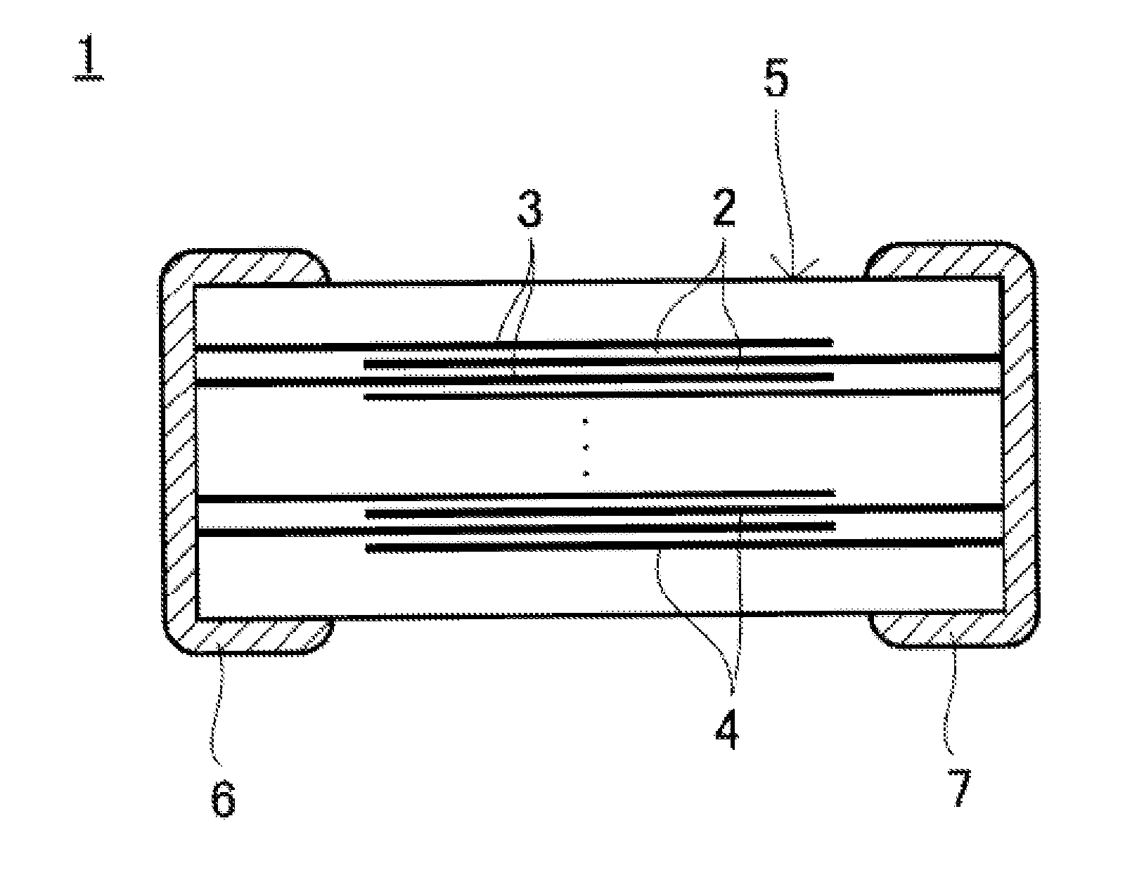
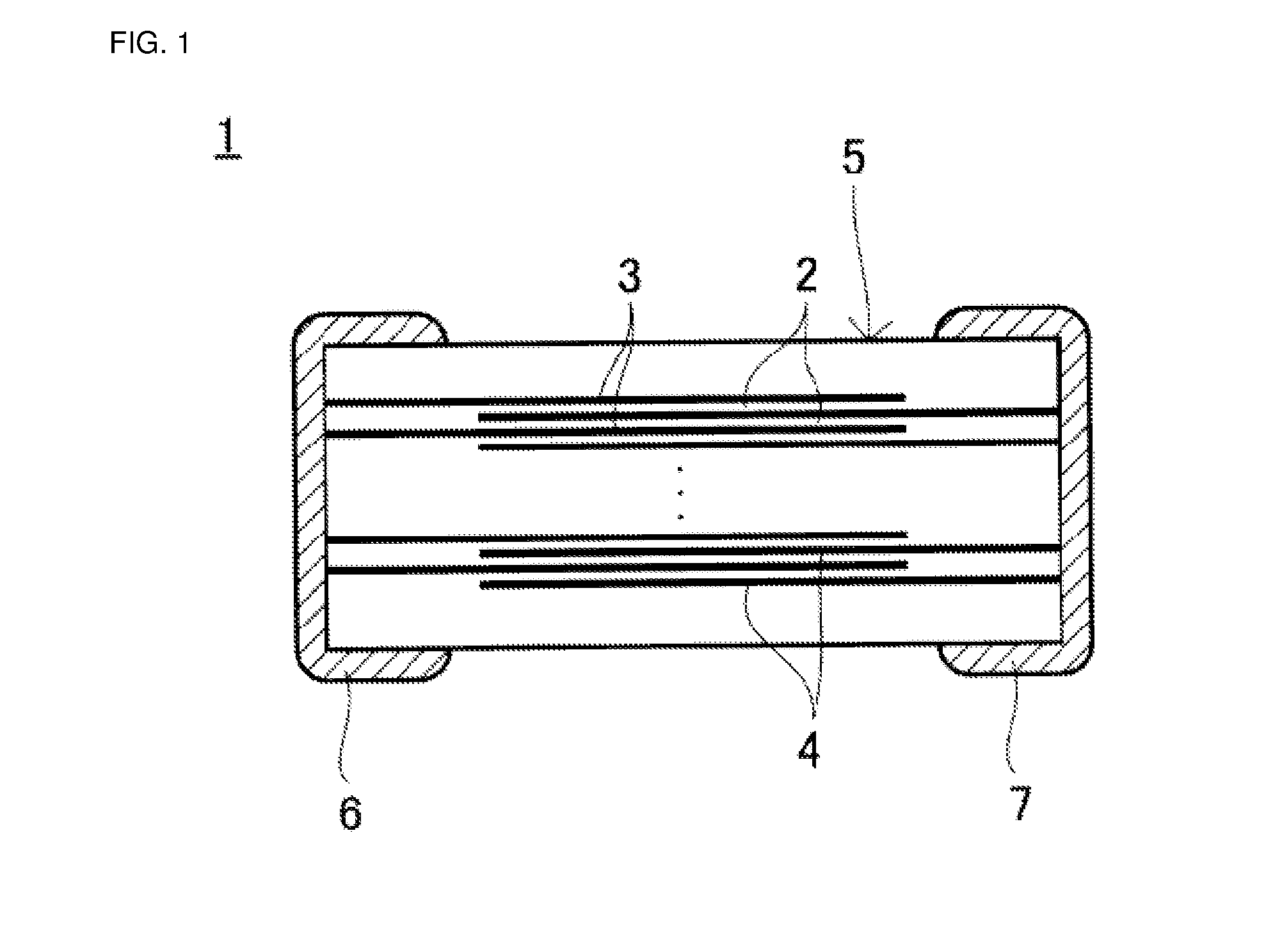
Image

Examples
experimental example 1
(A) Preparation of Ceramic Powder
[0027]Respective powders of particulate BaCO3, CaCO3, TiO2, Re (Re is La, Ce, Pr, Nd, Sm, Eu, Gd, Tb, Dy, Ho, Er, Tm, Yb, Lu and Y), and M (M is Mg, Mn, Al, Cr and Zn) were prepared as starting raw materials. Respective powders of La2O3, Ce2O3, Pr2O3, Nd2O3, Sm2O3, Eu2O3, Gd2O3, Tb2O3, Dy2O3, Ho2O3, Er2O3, Tm2O3, Yb2O3, Lu2O3, and Y2O3 were prepared as the Re powder. In addition, respective powders of MgCO3, MnCO3, Al2O3, Cr2O3, and ZnO were prepared as the M powder. Then, these powders were weighed for the composition of (Ba1-x-yCaxRey)(Ti1-zMz)O3 in Table 1, and then mixed for 80 hours in a ball mill. Thereafter, the mixed powders were subjected to a heat treatment at 1000° C. for calcination synthesis, thereby providing a main constituent powder of the formula (Ba1-x-yCaxRey)(Ti1-zMz)O3. Thereafter, 1.5 parts by mol of BaCO3 and 2 parts by mol of SiO2 were added to 100 parts by mol of the main constituent powder to obtain a ceramic powder.
[0028]Th...
experimental example 2
[0044]The influence of impurities was evaluated in Experimental Example 2. There is a possibility that Sr, Zr, Hf, Zn, Na, Ag, Pd, Ni, and the like will be present as impurities in a raw material preparation step, etc. for the laminated ceramic capacitor. These have the possibility of being present in the crystal grains and at crystal grain boundaries between crystal grains. In addition, there is a possibility that an internal electrode constituent will be diffused into crystal grain boundaries in the dielectric ceramic and crystal grain boundaries between crystal grains in a firing step, etc. for the laminated ceramic capacitor. Experimental Example 2 is intended to evaluate the influence of these impurities.
(A) Preparation of Ceramic Powder
[0045]Ceramic powders were prepared in the same way as in Experimental Example 1, except that the impurity components shown in Table 3 were added to the composition of sample number 13 in Experimental Example 1.
TABLE 3SampleNumberDetails of Impu...
PUM
| Property | Measurement | Unit |
|---|---|---|
| grain size | aaaaa | aaaaa |
| grain size | aaaaa | aaaaa |
| grain size | aaaaa | aaaaa |
Abstract
Description
Claims
Application Information
 - Generate Ideas
- Intellectual Property
- Life Sciences
- Materials
- Tech Scout
- Unparalleled Data Quality
- Higher Quality Content
- 60% Fewer Hallucinations
Browse by: Latest US Patents, China's latest patents, Technical Efficacy Thesaurus, Application Domain, Technology Topic, Popular Technical Reports.
© 2025 PatSnap. All rights reserved.Legal|Privacy policy|Modern Slavery Act Transparency Statement|Sitemap|About US| Contact US: help@patsnap.com