Integrated plasmonic nanocavity sensing device

a sensing device and nanocavity technology, applied in the field of integrated plasmonic devices, can solve the problems of limited dimensions of sensors, less attractive integration with silicon based electronic components, and constraints

Inactive Publication Date: 2013-06-13
INTEGRATED PLASMONICS CORP
View PDF3 Cites 16 Cited by
  • Summary
  • Abstract
  • Description
  • Claims
  • Application Information

AI Technical Summary

Benefits of technology

[0009]The structure of the integrated plasmonic sensing device allows dense integration of active plasmonic devices such as optical sources and optical detectors together with plasmonic elements such as waveguides and nanocavity resonators. Plasmonic nanocavity resonators are optical resonators constructed from combinations of dielectric and metallic materials that support electromagnetic modes at resonance frequencies corresponding to free-space wavelengths between approximately 200 nm and 2 um, in which the mode volume is less than approximately 1 cubic free-space wavelength. Moreover, the structure is compatible with CMOS architectures.
[0010]In one embodiment said plasmonic sensing device may comprise a nanocavity, wherein the electromagnetic fields supported by said nanocavity at resonance extend at least a part into the detection region of said detector such that the coupling between said plasmon resonances and said optical detector is maximized.

Problems solved by technology

While such sensors will typically meet sensitively requirements for useful sensors, their dimensions are limited by diffraction effects in the dielectric waveguide components used and by the coherence length of surface plasmon polaritons, which limits the area on a metal surface that can considered to represent an independent measurement.
Such sensors can be therefore less attractive for integration with silicon based electronic components, which are many times smaller.
One problem with EOT plasmonic sensing devices is that they will be subject to constraints deriving from the coherence length of single interface propagating surface plasmons, which is typically of the order of a few micrometers.
A second problem with such devices is that they will require at least two scattering centers to establish the interference condition necessary for EOT.
Hence in order to accomplish EOT effects typically an EOT-supporting metallic grating (e.g. an array of plasmonic scattering centers provided in a metallic layer or multilayer) of relatively large dimensions is needed so that a high integration density cannot be accomplished.
Such particles however are irregularly shaped and thus not very well defined resulting in deterioration of the resonant response of the sensor.
Moreover, the irregularly will also affect the uniformity of the sensors when fabricated as dense sensor arrays on a wafer.

Method used


Image

  • Integrated plasmonic nanocavity sensing device
  • Integrated plasmonic nanocavity sensing device
  • Integrated plasmonic nanocavity sensing device

Examples


Embodiment Construction

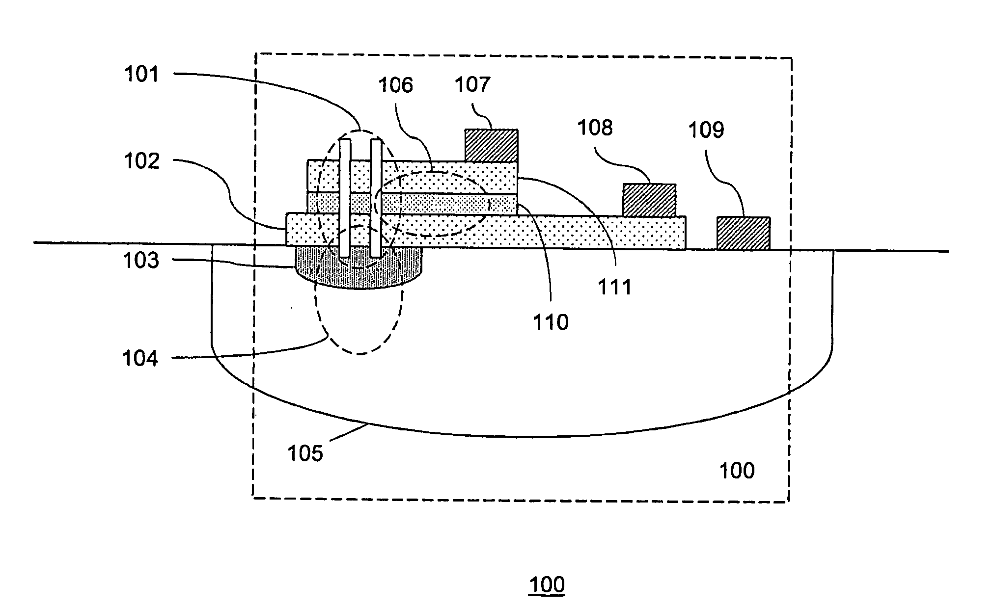
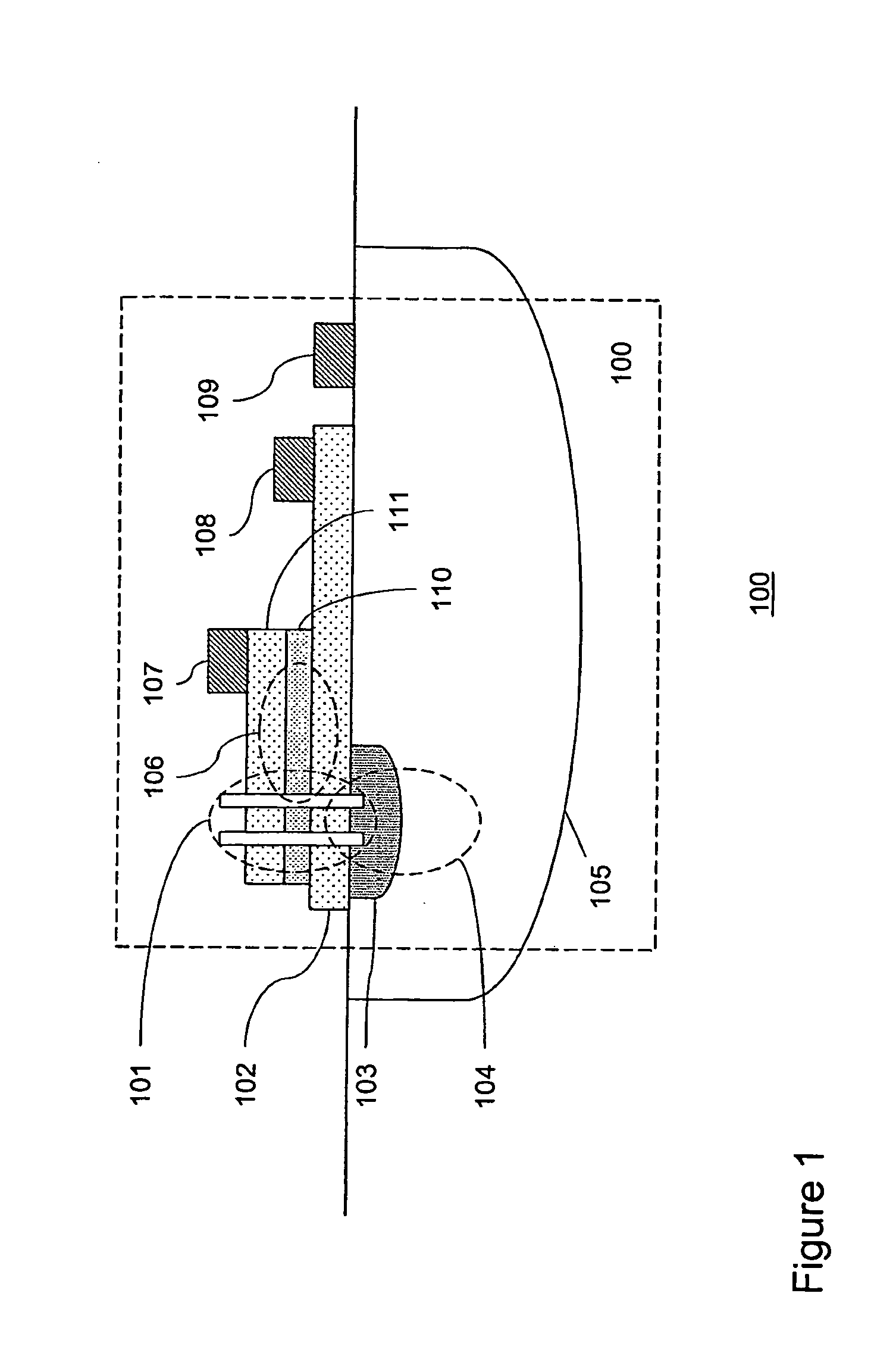
[0027]FIG. 1 is a schematic diagram showing a cross section of an integrated plasmonic sensing device 100 according to one embodiment of the invention. The integrated device may comprise a plasmonic nanocavity resonator 101, i.e. a sub-micron sized cavity configured for supporting localized resonant plasmonic modes inside the cavity, combined with an integrated optical source 106 and an integrated detector 104. In this non-limiting example, the resonant cavity 101 may be driven by the optical source 106, in particular guided surface plasmons generated by said optical source. To that end, the optical source 106 may comprise a conductive top and bottom layers 111, 102 forming the electrical contacts of the source. The conductive layers may relate to thin-film metal layers, in particular low-resistance thin-film metal layers, such as aluminum, copper, silver or gold having thickness within the range between 5 and 500 nm. In the example of FIG. 1 the conductive top layer may relate to a...


PUM

PropertyMeasurementUnit
wavelengthsaaaaaaaaaa
thicknessaaaaaaaaaa

Abstract

An integrated plasmonic sensing device is described wherein the integrated device comprises: at least one optical source comprising a first conductive layer and a second conductive layer, and a optical active layer between at least part of said first and second conductive layers; at least one nanocavity extending through said first and second conductive layers and said optical active layer, wherein said optical source is configured to generate surface plasmon modes suitable for optically activating one or more resonances in said nanocavity; and, at least one optical detector comprising at least one detection region formed in said substrate in the vicinity of said nanocavity resonator, wherein said optical detector is configured to sense optically activated resonances in said nanocavity.

Description

FIELD OF THE INVENTION[0001]The invention generally relates to integrated plasmonic devices and, in particular, though not necessarily, to an integrated plasmonic nanocavity sensing device and a plasmonic sensor pixel array comprising such devices.BACKGROUND OF THE INVENTION[0002]Many existing biological and chemical sensors detect the presence or absence of target material in the vicinity of the sensor based on changes in the propagation of electro-magnetic radiation. Such sensors have previously been fabricated using dielectric waveguide components on the basis of silicon-on-insulator (SOI) wafers and using metallic surfaces that support surface plasmon polaritons, i.e. electromagnetic excitations at a metal-dielectric interface. While such sensors will typically meet sensitively requirements for useful sensors, their dimensions are limited by diffraction effects in the dielectric waveguide components used and by the coherence length of surface plasmon polaritons, which limits the...

Claims


Application Information

Patent Timeline
Patent Type & Authority Applications(United States)
IPC IPC(8): G01N21/55
CPCB01L3/502715G01N21/55B01L2300/0663B82Y20/00G01N21/554G01N21/6454G01N21/648G01N21/6489G01N21/7746G01N2021/7776G01N2021/7786G01N2021/7789G02B6/1226H01L31/125B01L2300/0654
Inventor WALTERS, ROBERTSCHMITZ, JURRIAANPOLMAN, ALBERTBRUNETS, IHOR
Owner INTEGRATED PLASMONICS CORP
Why Eureka
Try Eureka