Sensor with vacuum cavity and method of fabrication

a vacuum cavity and sensor technology, applied in the direction of fluid pressure measurement by electric/magnetic elements, measurement devices, instruments, etc., can solve the problems of limited performance and/or complicated manufacturing process of conventional electronic devices such as microelectromachanical absolute pressure sensors, process is more complicated and expensive than a standard cmos process, and the accuracy of the roughness of the cavity surface is limited. , to achieve the effect of high capacitance density, low cost and high volum

Inactive Publication Date: 2013-06-20
URVAS ILKKA +2
View PDF3 Cites 18 Cited by
  • Summary
  • Abstract
  • Description
  • Claims
  • Application Information

AI Technical Summary

Benefits of technology

[0007]Briefly according to the present invention, a MEMS pressure sensing device has cavities with vertical height in nanometer scale that are manufactured with conventional thin film processing equipment such as those used in a CMOS foundry. The present invention enables the design of low cost, high volume devices with vacuum cavities within the chip. A typical device has a membrane that functions as the sensing element of the transducer. The membrane is formed by creating a vacuum cavity below the surface layer of the carrier, e.g. a CMOS chip. The transducer generates an output electrical signal that is proportional to the pressure affecting the sensing element. The sensing of the transducer can be based on either a change in capacitance or change in conductivity associated with electron tunneling current in the transducer, or the combination of both. In order to provide an output signal the device may require an input signal that is typically a DC, AC or modulated voltage or current.
[0008]The present invention provides means to produce a transducer where the moving membrane is separated from the bottom of the cavity by a very short distance in the order of nanometers to hundreds of nanometers. If the transducer is using capacitive sensing, this short distance enables a very high capacitance density and high change in capacitance for a given displacement of the sensor element, which results in improved sensitivity, and reduced area requirements for a given capacitance value. The possibility of using separation distance in the order of nanometers enables transducer structures where electron tunneling occurs between electrodes that are separated by the vacuum cavity. In this case a DC input signal can be used to generate a DC output signal that is very sensitive to the movement of the membrane. The use of DC signals simplifies the requirements of measurement electronics. In addition to the capacitive and electron tunneling based sensing it is also possible to use piezoresistive sensing; here the main benefit is related to the simplified process technology in making the cavity, since the small height of the cavity does not bring additional benefits to the sensing mechanism.

Problems solved by technology

Conventional electronic devices, such as microelectromachanical (MEMS) absolute pressure sensors, have a limited performance and / or complicated manufacturing process with the existing technologies.
In addition, the system requires a complicated package for two chips and additional input and output interfaces on both chips to transfer the signals between them.
However, the process is more complicated and expensive than a standard CMOS process due to the necessary MEMS processing steps.
The etching process is complicated and results in limited accuracy in the roughness of the cavity surfaces, in addition the minimum height of the cavity is limited with this method.
As this processing step is not compatible with standard CMOS technology, it requires a dedicated foundry which complicates the second sourcing of such technologies and limits the availability of this kind of solutions especially for fabless semiconductor companies.
The piezoresistive sensors have relatively large power consumption, strong temperature dependency and a limited accuracy due to the resistor based thermal noise.
The capacitive sensors have relatively low power consumption and a very low noise floor level, but require more complex measurement electronics and are sensitive to parasitic capacitance.

Method used


Image

  • Sensor with vacuum cavity and method of fabrication
  • Sensor with vacuum cavity and method of fabrication
  • Sensor with vacuum cavity and method of fabrication

Examples


first embodiment

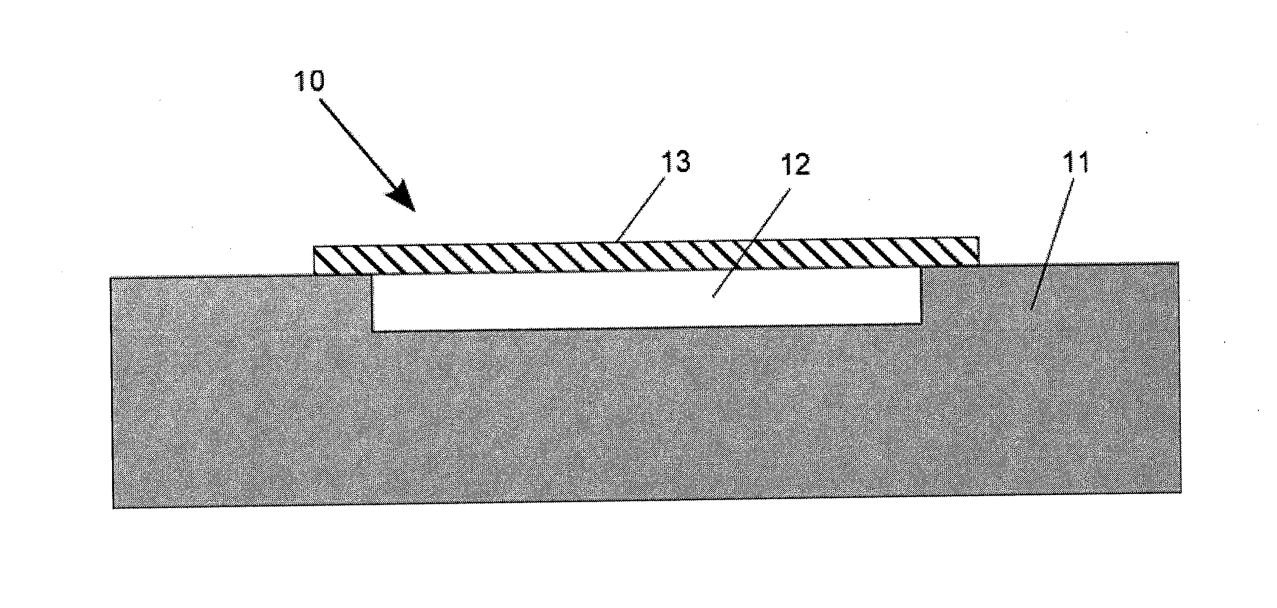
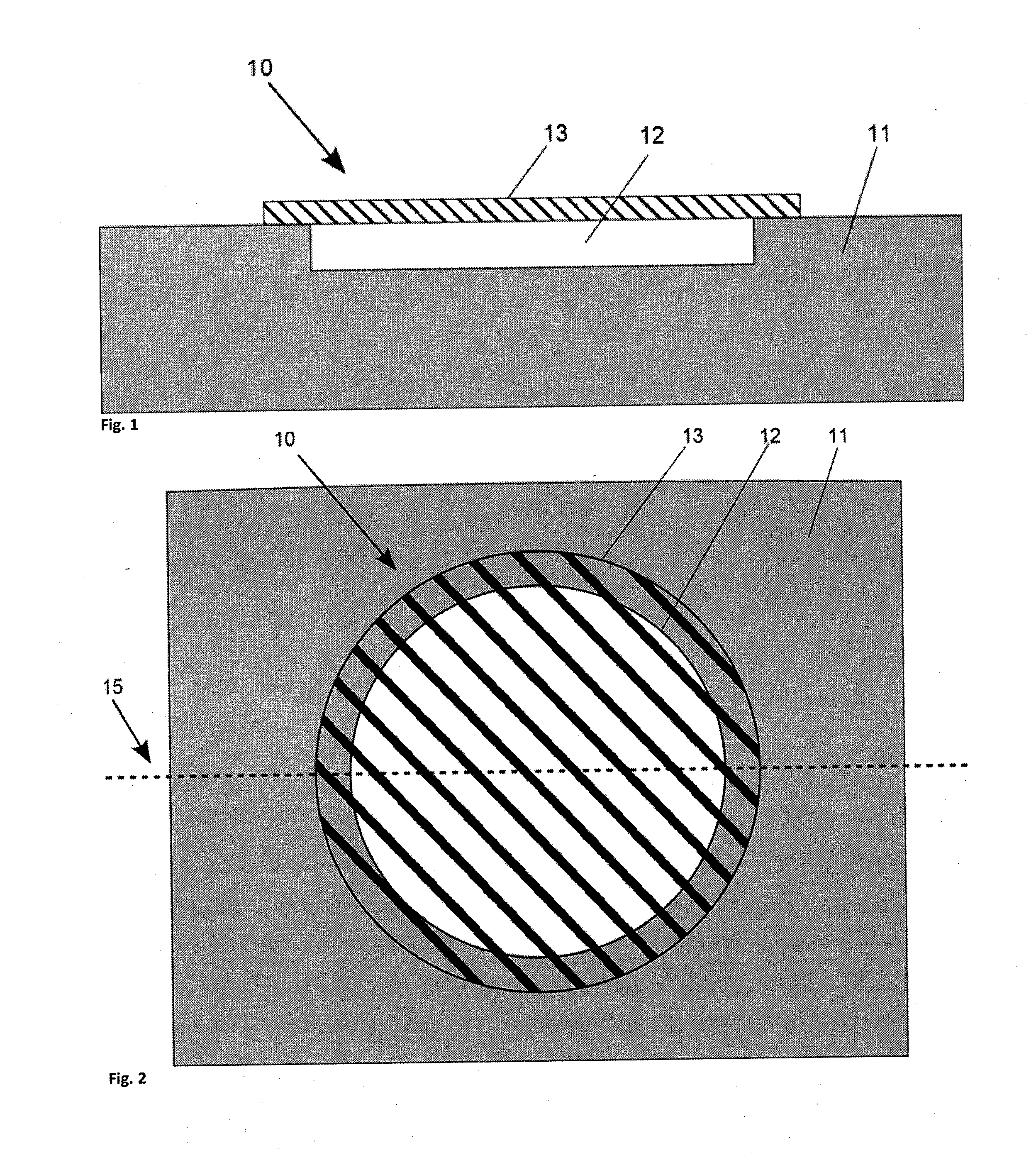
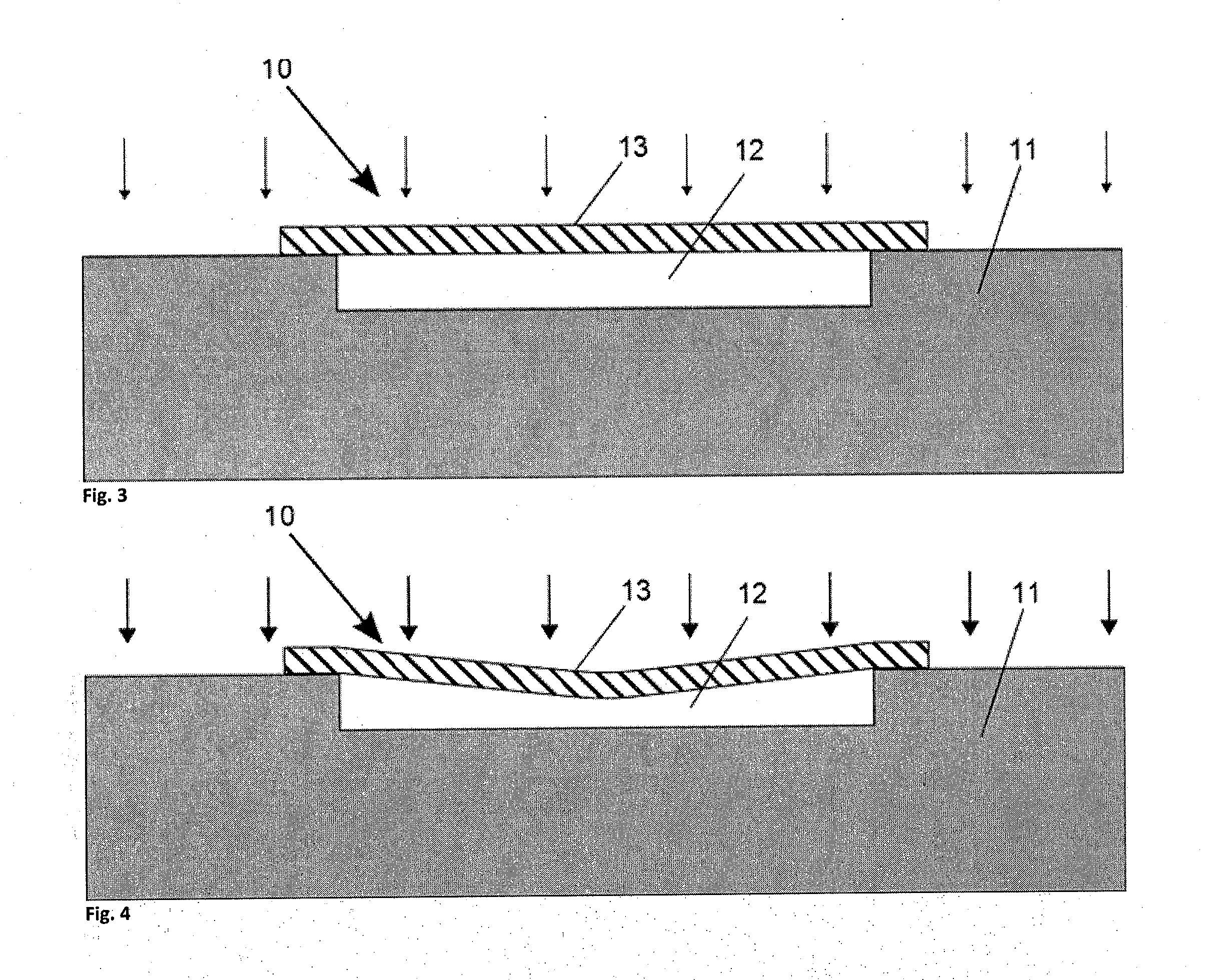
[0033]Referring now to the invention in more detail, in FIG. 1 and FIG. 2 there is shown a pressure sensor device 10 having a sensor element 13 that is on the top of the carrier 11 and the cavity 12. The sensor element 13 is covering the cavity 12 area so that it is hermetically sealed. The location of cross-section that is used for FIG. 1 is shown by the dashed line 15 in FIG. 2 that represents the top view of the device. Pressure sensor device 10 is used to describe the mechanical actuation of the sensor element 13, for this reason the other parts of the transducer are omitted.

[0034]The deformation of the sensor element 13 of pressure sensor device 10 is shown as a sequence in FIG. 3 to FIG. 7. In the figures eight down pointing arrows are used to depict the ambient pressure. In FIG. 3 the ambient pressure is very low, i.e. essentially the same as in the cavity 12. As a result the sensor element is not deformed by a pressure difference between the cavity and the ambient medium of ...

second embodiment

[0036]Referring now to the invention, in FIG. 8, FIG. 9 and FIG. 10 there is shown a pressure sensor device 20 having a sensor element 24 that is on the top of the carrier 21 and the cavity 23. The sensor element 24 is covering the cavity 23 area so that it is hermetically sealed. The bottom of the cavity 23 is covered by an electrode 22 that forms a capacitor i.e. the transducer together with the sensor element 24. In FIG. 8 the ambient pressure is minimal, therefore the sensor element 24 is not deformed and the capacitance of the pressure sensor device 20 is at its minimum. In FIG. 9 the ambient pressure is increased and as a consequence the sensor element 24 is deformed increasing the capacitance of the device. In FIG. 10 the ambient pressure is high enough to bring the sensor element 24 into a physical contact with the electrode 22. This can be detected as a short circuit of the transducer, which can be used to define the touching point of the pressure sensor device 20.

third embodiment

[0037]Referring now to the invention, in FIG. 11, FIG. 12 and FIG. 13 there is shown a pressure sensor device 30 having a sensor element 34 that is on the top of the carrier 31 and the cavity 33. The sensor element 34 is covering the cavity 33 area so that it is hermetically sealed. Below the cavity 33 embedded in the carrier 31 there is the electrode 32 that forms a capacitor i.e. the transducer together with the sensor element 34. In FIG. 11 the ambient pressure is minimal, therefore the sensor element 34 is not deformed and the capacitance of the pressure sensor device 30 is at its minimum. In FIG. 12 the ambient pressure is increased and as a consequence the sensor element 34 is deformed increasing the capacitance of the device. In FIG. 13 the ambient pressure is high enough to bring the center of the sensor element 34 into a physical contact with the carrier 31. However, as this part of the carrier 31 is made of an insulating material, there will not be short circuit between th...


PUM

PropertyMeasurementUnit
dielectric constantaaaaaaaaaa
heightaaaaaaaaaa

Abstract

A MEMS pressure sensor device comprises a sensor element positioned on top of a carrier and a cavity. The sensor element hermetically seals the cavity. An electrode is coupled to the cavity that forms a pressure transducer together with the sensor element. The cavity is created by a density changing material.

Description

CROSS-REFERENCE TO RELATED APPLICATIONS[0001]This application claims priority from U.S. patent application No. 61 / 554,212, filed Nov. 1, 2011, and is related to U.S. patent application Ser. No. 12 / 370,882 titled “Resonant MEMS device that detects photons, particles and small forces,” Ser. No. 12 / 961,079 titled “Electromechanical systems, waveguides and methods of production,” 61 / 388,481 titled “Method for fabrication of deep vacuum gap cavities inside materials,” 61 / 417537 titled “Metal and semiconductor nanotubes and hollow wires and method for their fabrication”, all of which are hereby incorporated by reference in their entirety.TECHNICAL FIELD[0002]The present invention is in the technical field of integrated thin film devices. More particularly, the present invention is in the technical field of microelectromechanical (MEMS) devices.BACKGROUND OF THE INVENTION[0003]Pressure sensing devices are known. Examples of such devices are described in U.S. Pat. No. 3,858,097 titled “PRES...

Claims


Application Information

Patent Timeline
Patent Type & Authority Applications(United States)
IPC IPC(8): G01L9/00
CPCG01L9/0073G01L9/0048
Inventor URVAS, ILKKAPAVLOV, ANDREI JURIEVICHPAVLOVA, YELENA VASILJEVNA
Owner URVAS ILKKA
Why Eureka
Try Eureka