
In-situ pre-clean prior to epitaxy

a technology of epitaxy and pre-cleaning, applied in the field of methods for cleaning the surface of semiconductors, can solve the problems of reducing the tolerance for imperfections in semiconductor processing, reducing the size of the semiconductor, and so as to reduce heating and process time, the effect of reducing the thermal load consumed and reducing the heating and process tim

Active Publication Date: 2013-06-20
ASM IP HLDG BV
View PDF7 Cites 3 Cited by
  • Summary
  • Abstract
  • Description
  • Claims
  • Application Information

AI Technical Summary

Benefits of technology

The patent describes a method for cleaning wafers using a low temperature process. This lowers the thermal load on the wafer, resulting in faster processing and increased reactor throughput. After cleaning, the wafer is ready for the next step, which can be a low temperature epitaxial process. This method is particularly useful for processes carried out between 350-615°C and using Cl2 or HCl as the etchant. It reduces the time, energy, and thermal budget consumption of heating and cooling the substrate and process chamber in conventional hydrogen bake steps.

Problems solved by technology

Recent advances in miniaturization and attendant circuit density, however, have lowered tolerances for imperfections in semiconductor processing.
Contaminants at the substrate surface, such as naturally forming “native oxide” and carbon contaminants, interfere with the crystal structure and consequent electrical properties of each overlying layer as it is formed, resulting in a polycrystalline layer.
Nevertheless, there is always at least a risk of some oxidation.
Even when processed immediately after an HF last, residual oxygen on the substrate can be too high for subsequent epitaxial deposition, especially at low temperatures.
Such bake steps can be costly both from a wafer throughput and a thermal budget perspective.
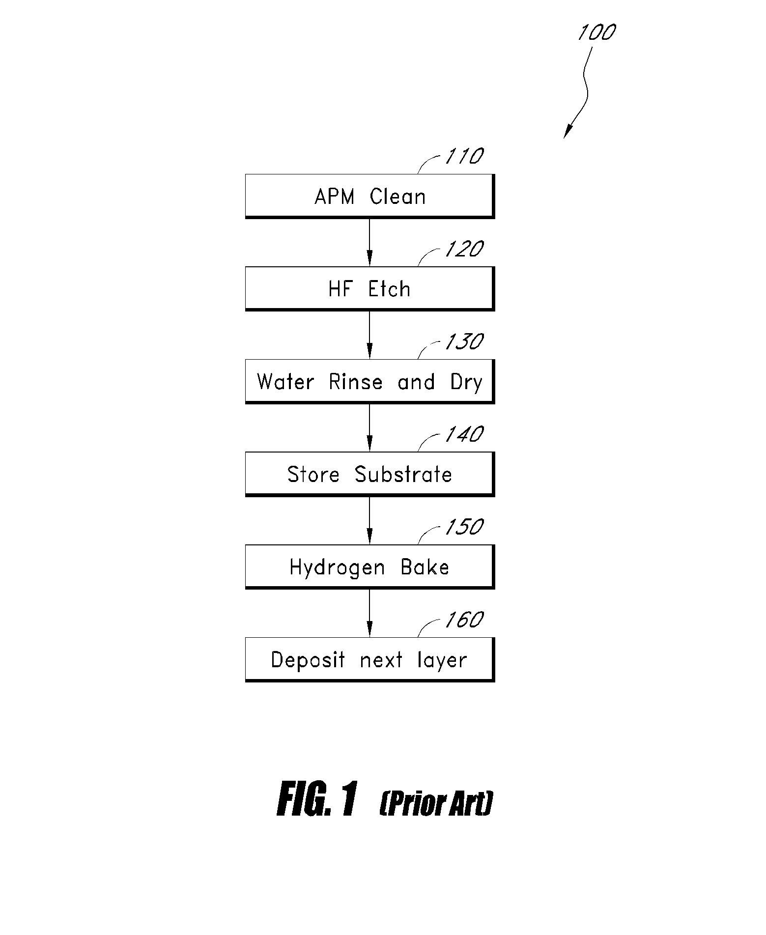
The problem of reoxidation after the HF last step has been detrimental to the high-throughput manufacturing of many silicon devices, but has been a particular hindrance in the deposition of epitaxial layers.

Method used


Image

  • In-situ pre-clean prior to epitaxy
  • In-situ pre-clean prior to epitaxy
  • In-situ pre-clean prior to epitaxy

Examples


example 1

[0069]FIG. 6 illustrates a Secondary Ion Mass Spectroscopy (SIMS) image of a cleaned silicon film on a substrate. The concentrations of oxygen and carbon are illustrated in atoms per cubic cm on the left y-axis and the germanium concentration is illustrated in atomic percent. The concentrations are plotted versus the depth of the sample substrate. To facilitate SIMS testing, an epitaxial silicon capping layer is deposited over the surface or film of interest to seal it for testing. Typically, the silicon capping layer is about 25 nm or thicker.

[0070]The silicon surface of the substrate was cleaned by providing GeH4 to react with native oxide present on the substrate surface, thereby forming some GeOx. Some of the GeOx compounds were removed by subsequently providing HCl. The process used to clean the interface in FIG. 6 was not optimized. Nevertheless, despite lack of optimization, the method left only approximately 8*1011 atoms per cm2 of oxygen.

[0071]The silicon capping layer for ...

example 2

[0073]FIG. 7 illustrates a SIMS image of a silicon film on a substrate cleaned by an optimized process comprising providing GeH4 and HCl.

[0074]The silicon capping layer for the sample analyzed in FIG. 7 was about 65 nm thick. The cleaned silicon surface of the sample tested in FIG. 7 is thus illustrated at a depth of about 65 nm. No spike in oxygen concentration is observed at the cleaned interface in FIG. 7. The SIMS measurement for oxygen at the cleaned silicon surface was below the lower SIMS detection limit for oxygen. Thus, the SIMS data shown in FIG. 7 indicates that substantially all of the oxygen is removed by the optimized cleaning process comprising providing GeH4 to form GeOx compounds and subsequently using HCl to remove the GeOx compounds.

[0075]Advantageously, the cleaning process used in FIG. 7 does not require a pre-epi temperature bake to remove or eliminate oxygen present on the surface of the substrate after the wet clean.


PUM

PropertyMeasurementUnit
temperatureaaaaaaaaaa

Abstract

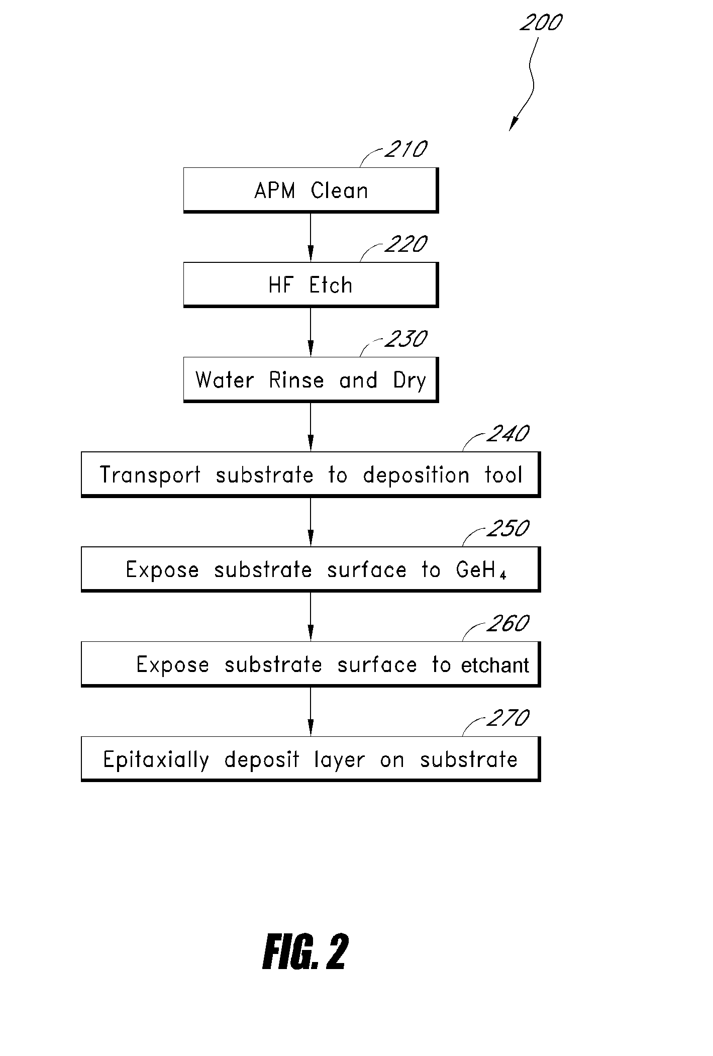
Methods for low temperature cleaning of a semiconductor surface prior to in-situ deposition have high throughput and consume very little of the thermal budget. GeH4 deposits Ge on the surface and converts any surface oxygen to GeOx. An etchant, such as Cl2 or HCl removes Ge and any GeOx and epitaxial deposition follows. A spike in Ge concentration can be left on the substrate from diffusion into the substrate. All three steps can be conducted sequentially in-situ at temperatures lower than conventional bake steps.

Description

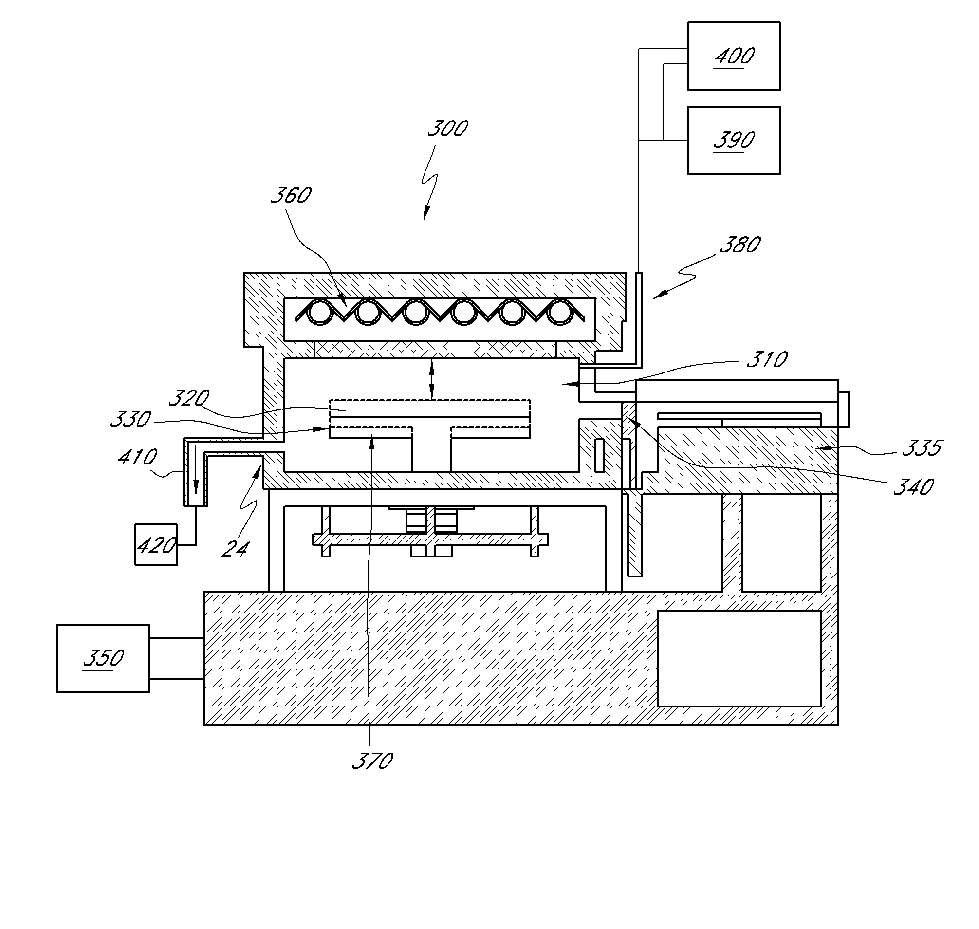
BACKGROUND OF THE INVENTION[0001]1. Field of the Invention[0002]This invention relates generally to methods for cleaning of a semiconductor surface, and relates more specifically to a method for low temperature, in-situ semiconductor cleaning in a deposition tool.[0003]2. Description of the Related Art[0004]High-temperature ovens, called reactors, are used to create structures of very fine dimensions, such as integrated circuits on semiconductor substrates. One or more substrates, such as silicon wafers, are placed on a wafer support inside the reaction chamber. Both the wafer and support are heated to a desired temperature. In a typical wafer treatment step, reactant gases are passed over the heated wafer, causing the chemical vapor deposition (CVD) of a thin layer of the reactant material on the wafer. Various process conditions, particularly temperature uniformity and reactant gas distribution, must be carefully controlled to ensure the high quality of the resulting layers.[0005]...

Claims


Application Information

Patent Timeline
Patent Type & Authority Applications(United States)
IPC IPC(8): H01L29/16B08B5/00H01L21/306H01L21/20
CPCH01L21/02381H01L21/02661H01L21/02532H01L21/302
Inventor CODY, NYLES W.THOMAS, SHAWN G.TOMASINI, PIERRE
Owner ASM IP HLDG BV
Learn More