Semiconductor device and method for manufacturing the same
Inactive Publication Date: 2013-06-27
SEMICON ENERGY LAB CO LTD
View PDF5 Cites 18 Cited by
Summary
Abstract
Description
Claims
Application Information
AI Technical Summary
This helps you quickly interpret patents by identifying the three key elements:
Problems solved by technology
Method used
Benefits of technology
Benefits of technology
The patent aims to improve the performance of a miniaturized transistor by improving its on-state characteristics, such as current or field-effect mobility, to achieve high-speed response and operation. The invention provides a structure of a semiconductor device and a manufacturing method to achieve this goal.
Problems solved by technology
Further, in accordance with miniaturization of the transistor, concern about a decrease in yield of a manufacturing process rises.
Method used
Image
Click on the blue label to locate the original text in one second.
Reading with bidirectional positioning of images and text.
Examples
embodiment 1
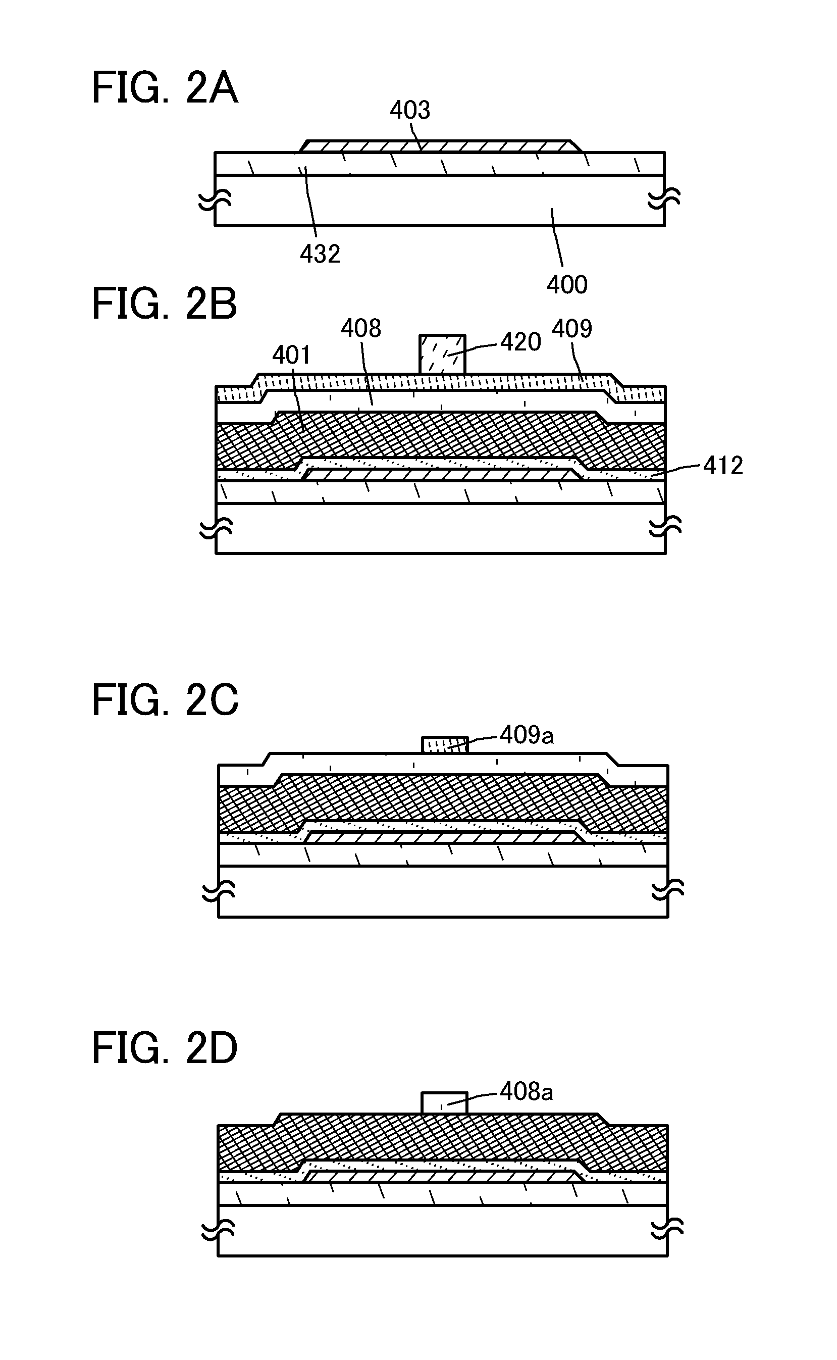
[0054]In this embodiment, one embodiment of a semiconductor device and a method for manufacturing the semiconductor device, which is one embodiment of the present invention, will be described with reference to FIGS. 1A and 1B, FIGS. 2A to 2D, FIGS. 3A to 3D, and FIGS. 4A to 4D.
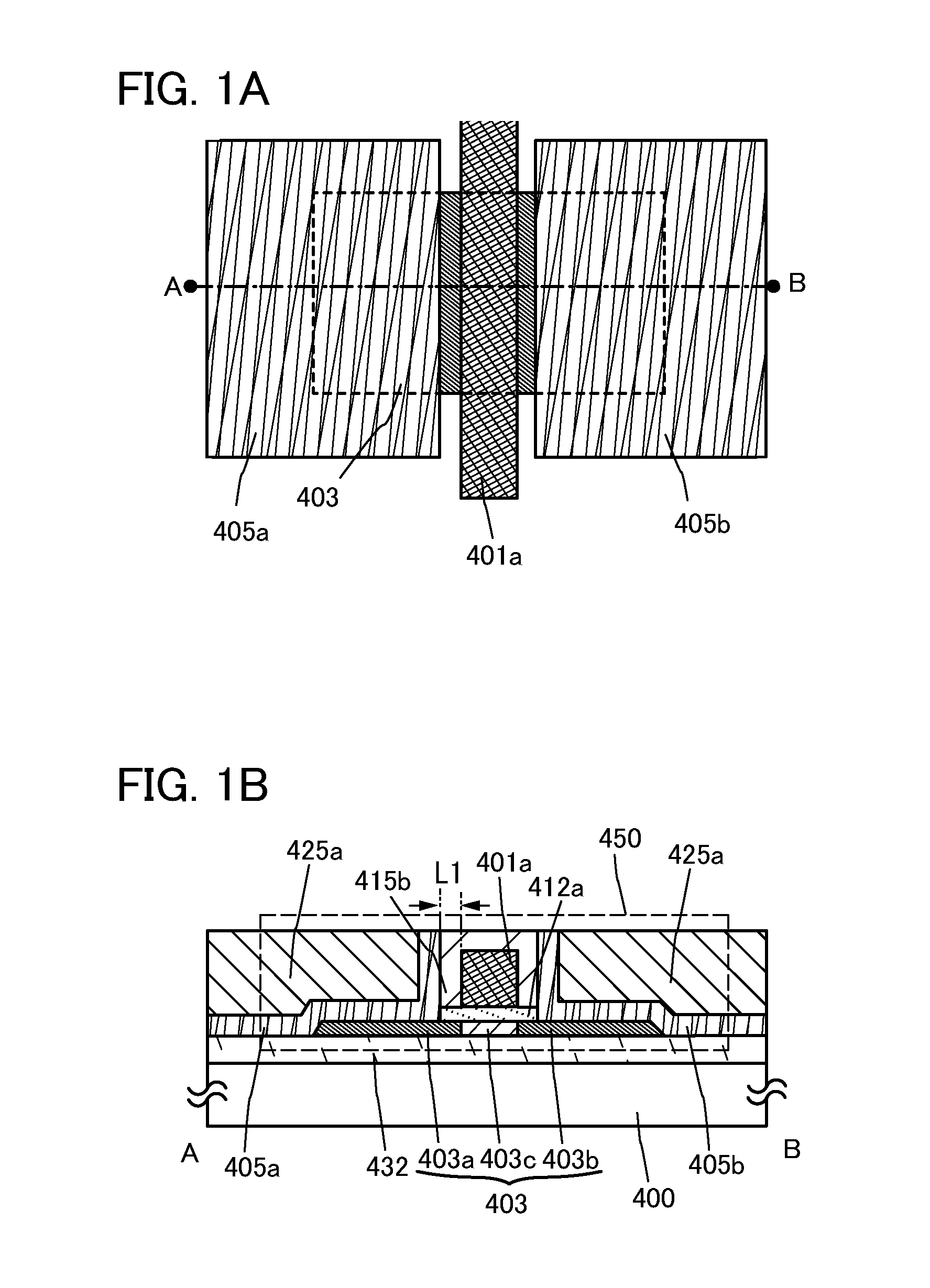
[0055]FIGS. 1A and 1B are a plan view and a cross-sectional view of a transistor 450. FIG. 1A is a plan view and FIG. 1B is a cross-sectional view taken along line A-B in FIG. 1A. Note that in FIG. 1A, some components (e.g., a base insulating film 432) of the transistor 450 are omitted to avoid complexity.
[0056]FIGS. 1A and 1B are an example of a structure of a semiconductor device manufactured according to a method of this embodiment. The transistor 450 illustrated in FIGS. 1A and 1B includes a base insulating film 432 provided over a substrate 400 having an insulating surface, an oxide semiconductor film 403 including a channel formation region 403c and low-resistance regions 403a and 403b with the channel f...
embodiment 2
[0160]In this embodiment, a structure of a semiconductor device in one embodiment of the present invention, which is different from that in Embodiment 1, will be described.
[0161]FIGS. 5A and 5B are a plan view and a cross-sectional view of a transistor 470. FIG. 5A is a plan view and FIG. 5B is a cross-sectional view taken along line C-D in FIG. 5A. Note that in FIG. 5A, some components (e.g., a base insulating film 432) of the transistor 470 are omitted to avoid complexity.
[0162]Note that, in this embodiment, portions that are similar to the portions in Embodiment 1 are denoted by the same reference numerals in the drawings, and detailed description thereof is omitted.
[0163]FIGS. 5A and 5B are an example of a structure of a semiconductor device manufactured according to a method of this embodiment. The transistor 470 illustrated in FIGS. 5A and 5B includes a base insulating film 432 provided over a substrate 400 having an insulating surface, an oxide semiconductor film 403 includin...
embodiment 3
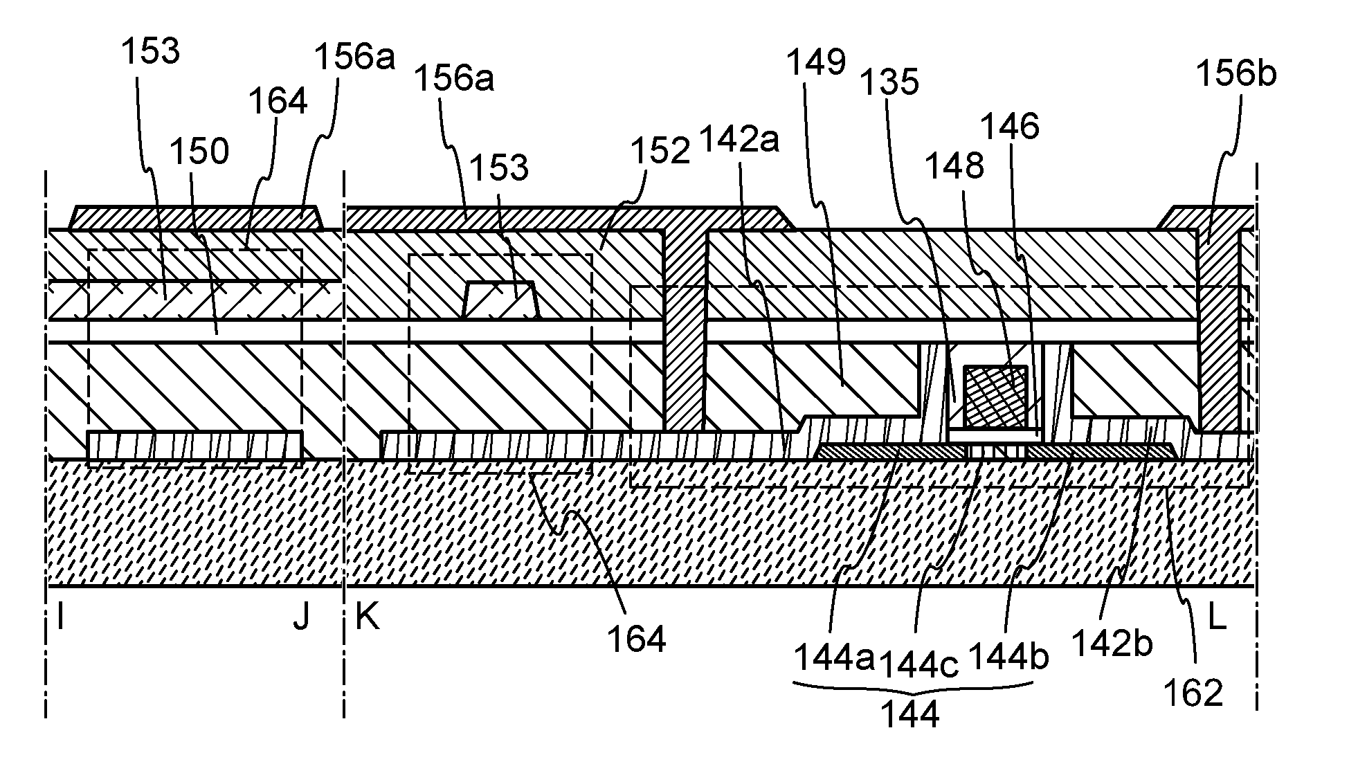
[0186]In this embodiment, an example of a semiconductor device which includes the transistor described in Embodiment 1, can hold stored data even when not powered, and does not have a limitation on the number of write cycles will be described with reference to drawings. Note that a transistor 162 included in the semiconductor device in this embodiment is the transistor 450 described in Embodiment 1.
[0187]FIGS. 6A to 6C illustrate an example of a structure of a semiconductor device. FIG. 6A is a cross-sectional view of the semiconductor device, FIG. 6B is a plan view of the semiconductor device, and FIG. 6C is a circuit diagram of the semiconductor device. Here, FIG. 6A corresponds to cross sections taken along line E-F and line G-H in FIG. 6B.
[0188]The semiconductor device illustrated in FIGS. 6A and 6B includes a transistor 160 including a first semiconductor material in a lower portion, and the transistor 162 including a second semiconductor material in an upper portion. The trans...
PUM
Abstract
A first conductive film overlapping with an oxidesemiconductor film is formed over a gate insulating film, a gate electrode is formed by selectively etching the first conductive film using a resist subjected to electron beam exposure, a first insulating film is formed over the gate insulating film and the gate electrode, removing a part of the first insulating film while the gate electrode is not exposed, an anti-reflective film is formed over the first insulating film, the anti-reflective film, the first insulating film and the gate insulating film are selectively etched using a resist subjected to electron beam exposure, and a source electrode in contact with one end of the oxidesemiconductor film and one end of the first insulating film and a drain electrode in contact with the other end of the oxidesemiconductor film and the other end of the first insulating film are formed.
Description
BACKGROUND OF THE INVENTION[0001]1. Field of the Invention[0002]The present invention relates to a semiconductor device and a method for manufacturing the semiconductor device.[0003]In this specification, a semiconductor device generally refers to a device which can function by utilizing semiconductor characteristics, and an electrooptic device, a semiconductor circuit, and electronic equipment are all semiconductor devices.[0004]2. Description of the Related Art[0005]Attention has been focused on a technique for forming a transistor using a semiconductor thin film formed over a substrate having an insulating surface (also referred to as a thin film transistor (TFT)). The transistor is applied to a wide range of electronic devices such as an integrated circuit (IC) or an image display device (display device). A silicon-based semiconductor material is widely known as a material for a semiconductor thin film applicable to a transistor. As another material, an oxide semiconductor has b...
Claims
Application Information
Patent Timeline
Application Date:The date an application was filed.
Publication Date:The date a patent or application was officially published.
First Publication Date:The earliest publication date of a patent with the same application number.
Issue Date:Publication date of the patent grant document.
PCT Entry Date:The Entry date of PCT National Phase.
Estimated Expiry Date:The statutory expiry date of a patent right according to the Patent Law, and it is the longest term of protection that the patent right can achieve without the termination of the patent right due to other reasons(Term extension factor has been taken into account ).
Invalid Date:Actual expiry date is based on effective date or publication date of legal transaction data of invalid patent.

