CMOS Device for Reducing Charge Sharing Effect and Fabrication Method Thereof

Active Publication Date: 2013-06-27
SEMICON MFG INT (SHANGHAI) CORP +1
View PDF7 Cites 8 Cited by
  • Summary
  • Abstract
  • Description
  • Claims
  • Application Information

AI Technical Summary

Benefits of technology

[0021]The present invention has porous material with dangling bonds disposed right below the isolation region, such as the additional isolation region of porous silicon. Since the porous silicon is a functional material of spongy structure formed by electrochemistry anodic oxidizing a monocrystalline silicon wafer, there are a large number of microvoids and dangling bonds on the surface of the porous silicon. These defects may form defect states in the forbidden band of the porous silicon, and the defect states may trap carriers so as to cause an increased

Problems solved by technology

When high energy charged ions from the aerospace or the ground pass through the integrated circuit element device, a large number of electron hole pairs deposited in the track are collected by sensitive nodes (i.e. reversed biased pn junctions) of the integrated circui

Method used


Image

  • CMOS Device for Reducing Charge Sharing Effect and Fabrication Method Thereof
  • CMOS Device for Reducing Charge Sharing Effect and Fabrication Method Thereof
  • CMOS Device for Reducing Charge Sharing Effect and Fabrication Method Thereof

Examples


Embodiment Construction

[0026]The embodiments of the present invention will now be illustrated in detail in conjunction with attached drawings.

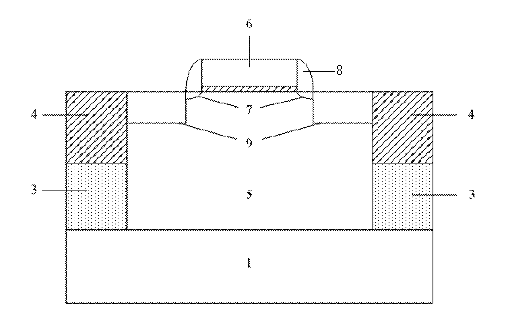
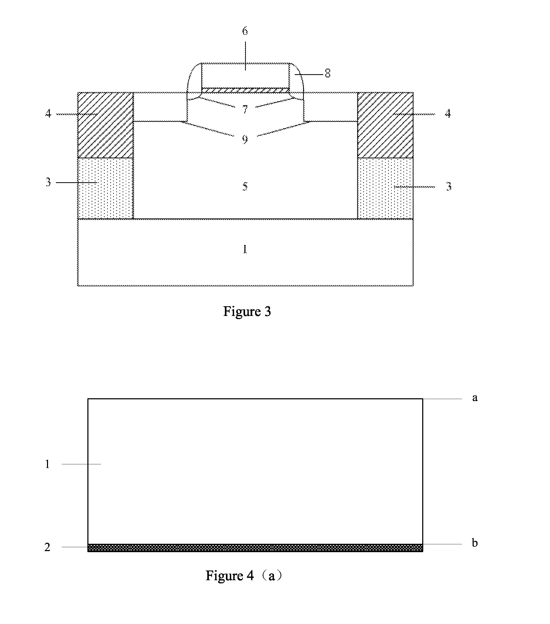
[0027]As shown in FIG. 2, a NMOS device is described as an example. Due to the ionization process produced by heavy ions, a large number of electron hole pairs will be formed along the track of the heavy ions. The holes move to the substrate, one portion of electrons are collected by sensitive nodes of the device to which the heavy ions are incident, and the other portion of electrons diffuse from a lower portion of an isolation region (e.g. STI region) to sensitive nodes of nearby devices and are collected. Therefore, an additional isolation region 3 of porous silicon material is disposed under the isolation region of the device, so that electrons or holes are trapped when diffusing toward nearby devices, the number of the electrons and the holes reaching the sensitive nodes of nearby devices is reduced, and thus the charge sharing effect can be effectively inhibit...


PUM


Abstract

The present invention discloses a CMOS device of reducing charge sharing effect and a fabrication method thereof. The present invention has an additional isolation for trapping carriers disposed right below an isolation region. the material of the additional isolation region is porous silicon. Since porous silicon is a functional material of spongy structure by electrochemistry anodic oxidizing monocrystalline silicon wafer, there are a large number of microvoids and dangling bonds on the surface layer of the porous silicon. These defects may form defect states in a center of forbidden band of the porous silicon, the defect states may trap carriers so as to cause an increased resistance. And with an increase of density of corrosion current, porosity increases, and defects in the porous silicon increase. The present invention can reduce the charge sharing effect due to heavy ions by using a feature that the defect states in the porous silicon trap carriers, the formation of a shallow trench isolation (STI) region and a isolation region underneath only needs one time photolithography, and the process is simple, so that radioresistance performance of an integrated circuit may be greatly increased.

Description

CROSS REFERENCE OF THE INVENTION[0001]The present application claims priority to Chinese application No. 201110436842.8, filed on Dec. 23, 2011, which is incorporated herein by reference.FIELD OF THE INVENTION[0002]The present invention relates to a CMOS device, particularly relates to a CMOS device for reducing a charge sharing effect in a radiation environment and a fabrication method thereof.BACKGROUND OF THE INVENTION[0003]With a continuous development of the semiconductor technology, the size of integrated circuit element device has been less than 100 nm. When high energy charged ions from the aerospace or the ground pass through the integrated circuit element device, a large number of electron hole pairs deposited in the track are collected by sensitive nodes (i.e. reversed biased pn junctions) of the integrated circuit element device, which causes an improper variation of logic states of the element device or damage to the element device. For conventional integrated circuit e...

Claims


Application Information

Patent Timeline
IPC IPC(8): H01L27/092H01L21/8238
CPCH01L21/823878H01L27/0921H01L21/3063H01L21/02216H01L21/02203
Inventor HUANG, RUTAN, FEIAN, XIAHUANG, QIANQIANYANG, DONGZHANG, XING
Owner SEMICON MFG INT (SHANGHAI) CORP
Why Eureka
Try Eureka