Charged particle beam lithography apparatus and method, and article manufacturing method

a lithography apparatus and a technology of chargeable particles, applied in the direction of photomechanical equipment, beam deviation/focusing by electric/magnetic means, instruments, etc., can solve the problems of inability to accurately write the pattern, difficulty in replacing the blanking deflector array, and inability to induce new failures

Inactive Publication Date: 2013-06-27
CANON KK
View PDF3 Cites 32 Cited by
  • Summary
  • Abstract
  • Description
  • Claims
  • Application Information

AI Technical Summary

Benefits of technology

[0008]The present invention provides, for example, a lithography apparatus that is advantageous for shielding of a charged particle beam that cannot be blanked.
[0010]According to the present invention, for example, a lithography apparatus that is advantageous for shielding charged particle beams which cannot be blanked may be provided.

Problems solved by technology

In the conventional multi beam lithography apparatus, if some portion, such as one where a beam defect occurs, of any one of the components relating to the writing ON / OFF state becomes uncontrollable after the start of operating the apparatus, a pattern cannot be written accurately.
However, multiple feed-power implementations need to be separated and a new failure may be induced in the course of replacement.
Furthermore, it becomes difficult to replace the blanking deflector array from the viewpoint of cost and time with increase in the number of beams for use.
On the other hand, the configuration of the charged particle beam exposure apparatus disclosed in Japanese Patent No. 4634076 with respect to electron beams in an unshielded state at all times is not preferred because the configuration of the apparatus becomes complicated due to the addition of a shutter mechanism so that normal electron beams located around electron beams in an unshielded state at all times are also blocked.

Method used


Image

  • Charged particle beam lithography apparatus and method, and article manufacturing method
  • Charged particle beam lithography apparatus and method, and article manufacturing method
  • Charged particle beam lithography apparatus and method, and article manufacturing method

Examples


Embodiment Construction

[0020]Hereinafter, preferred embodiments of the present invention will be described with reference to the drawings.

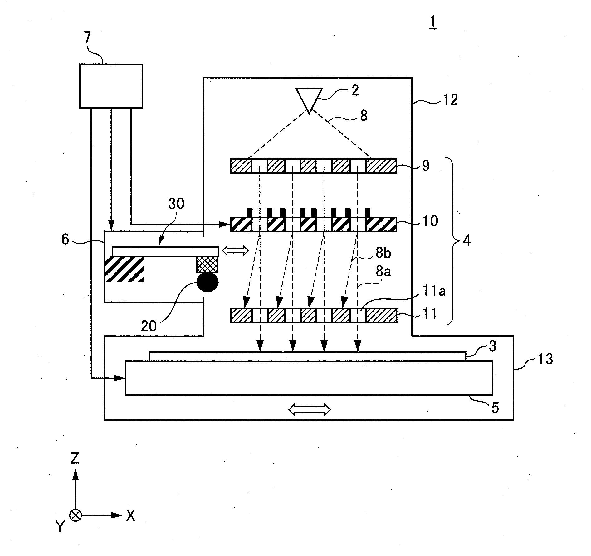
[0021]Firstly, a description will be given of a charged particle beam lithography apparatus (hereinafter referred to as “lithography apparatus”) according to one embodiment of the present invention. In particular, the lithography apparatus of the present embodiment is a lithography apparatus employing a multiple beam system in which a plurality of electron beams (charged particle beams) is deflected (scanned) and the blanking (OFF irradiation) of electron beams is independently controlled so as to write predetermined writing data at a predetermined position on a substrate to be treated. Here, a charged particle beam is not limited to an electron beam used in the present embodiment, but may be other charged particle beams such as an ion beam. FIG. 1 is a schematic diagram illustrating the configuration of a lithography apparatus 1 according to the present embodiment. In ...


PUM


Abstract

A lithography apparatus performs writing on a substrate with a plurality of charged particle beams and includes a blanking deflector array for blanking the plurality of charged particle beams; an aperture array configured to block a charged particle beam deflected by the blanking deflector array; and a sealing mechanism configured to seal an opening of at least one of the blanking deflector array and the aperture array with a shielding material that shields a charged particle beam.

Description

BACKGROUND OF THE INVENTION[0001]1. Field of the Invention[0002]The present invention relates to a charged particle beam lithography apparatus and method, and an article manufacturing method.[0003]2. Description of the Related Art[0004]Lithography apparatuses that perform writing on a substrate by controlling deflection scanning and blanking of charged particle beams such as electron beams are known. The lithography apparatuses may be employed as one of pattern forming technologies that is an alternative to optical exposure systems to produce logic LSI or other highly-integrated devices with a line width of 0.1 μm or less. Among the lithography apparatuses, there is a multi beam lithography apparatus that writes a pattern in parallel with a plurality of electron beams (charged particle beams). The multi beam lithography apparatus has a number of advantages for practical applications, such as unnecessary use of a mask (original plate) which is one of factors responsible for increasin...

Claims


Application Information

Patent Timeline
Patent Type & Authority Applications(United States)
IPC IPC(8): G21K5/04
CPCH01J37/09H01J2237/026H01J2237/0435B82Y40/00H01J37/3177G21K5/04B82Y10/00H01J2237/31794
Inventor YAMANAKA, TOSHIRO
Owner CANON KK
Why Eureka
Try Eureka