High-k metal gate random access memory
a random access memory and metal gate technology, applied in the field of random access memory, can solve the problems of reducing the size of the semiconductor component, affecting so as to achieve the effect of reducing the horizontal area of the transistor, increasing the component density, and maintaining the performance of the transistor
- Summary
- Abstract
- Description
- Claims
- Application Information
AI Technical Summary
Benefits of technology
Problems solved by technology
Method used
Image
Examples
embodiment 1
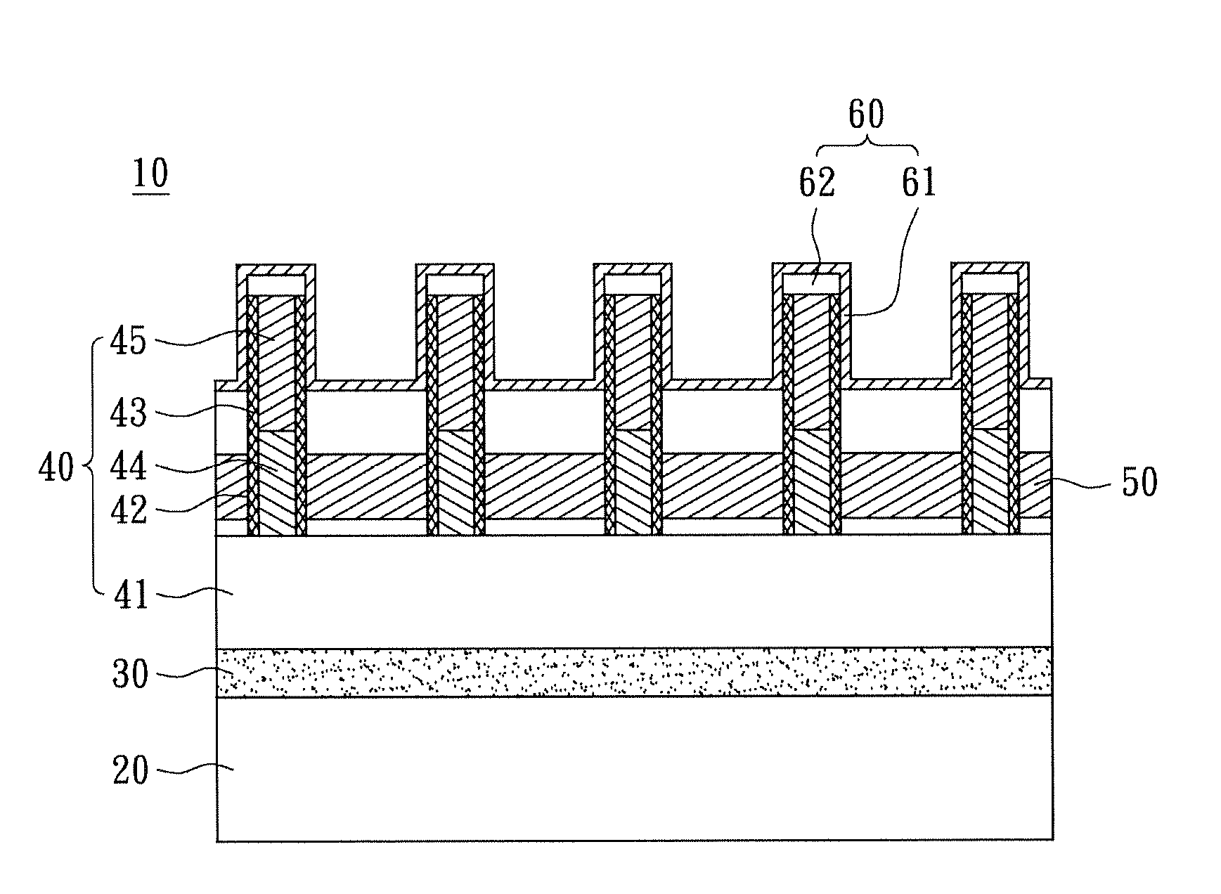
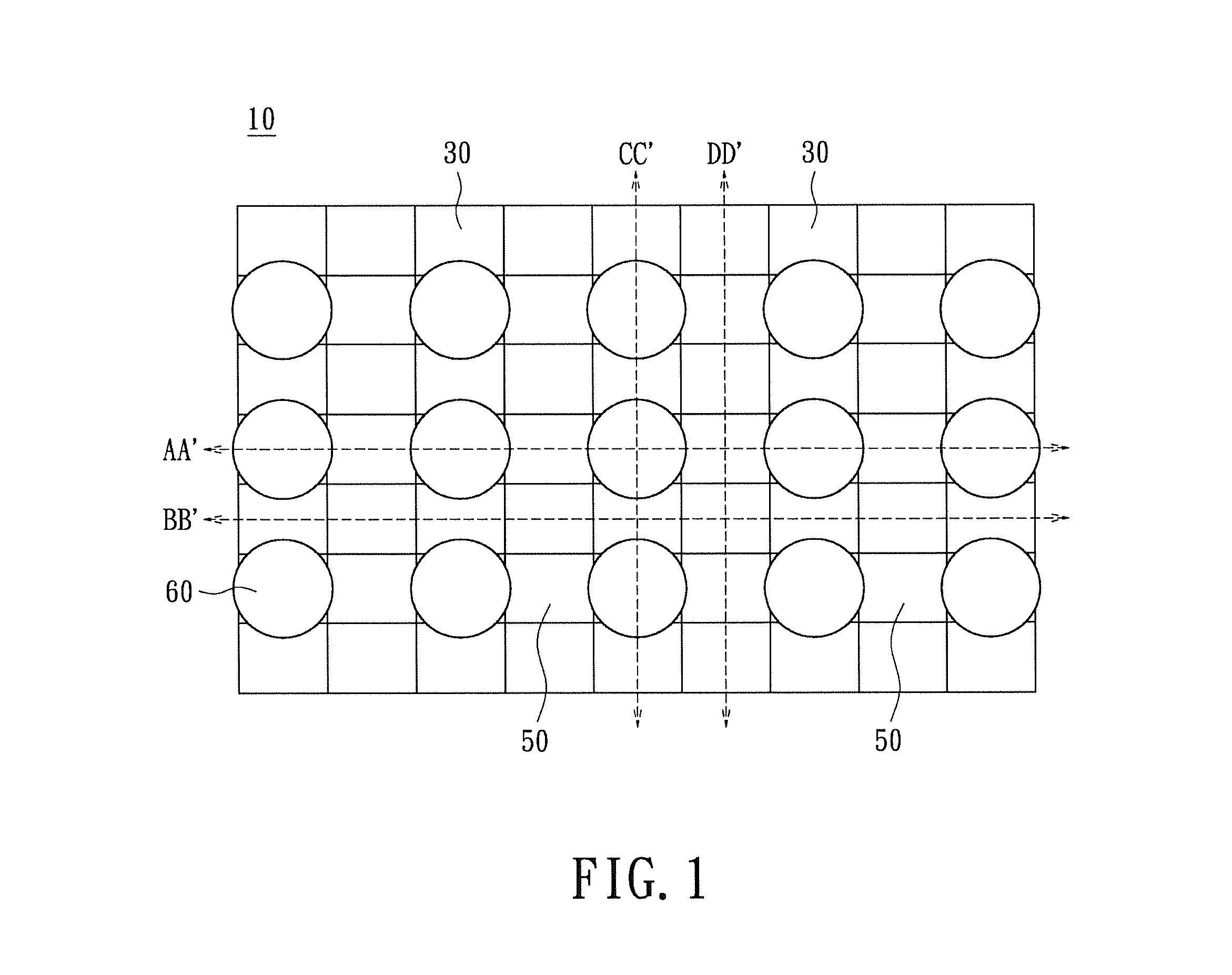
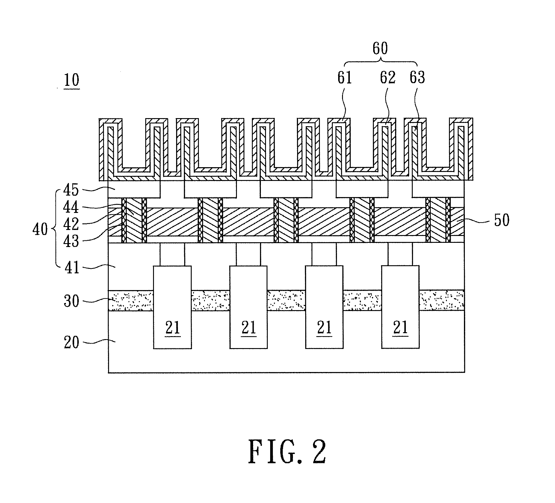
[0022]Please refer to FIG. 2, which shows a sectional view of the random access memory 10 in FIG. 1 taken along a cut-line AA′ for a first embodiment of the instant disclosure. The substrate 20 has a plurality of trenches 21 formed thereon, where the trenches 21 extend beyond the substrate 20. The trenches 21 are filled with insulating material such as silicon dioxide (silica), silicon nitride, borophosphosilicate glass (BPSG), phosphosilicate glass (PSG), undoped silicon glass (USG), or any material having high dielectric constant. However, the filler material is not restricted thereto. The bit line units 30 are arranged parallel at a distance from one another on the substrate 20. The bit line units 30 and the trenches 21 are alternately arranged on the substrate 20.
[0023]A plurality of high-k metal gate transistors 40 is disposed on the bit line units 30. Specially, the transistors 40 are perpendicular to the substrate 20, unlike the conventional ones which are parallel. Each of t...
embodiment 2
[0027]The instant disclosure further provides another high-k metal gate random access memory 10. Please refer to FIG. 6, where a sectional view of the random access memory 10 shown in FIG. 1 taken along the cut-line AA′ for the second embodiment is shown. The difference between the instant embodiment and the preceding embodiment is this: for the instant embodiment, each of the drain regions 45 and a portion of each gate structure 42 are arranged inside the respective capacitance unit 60. For this configuration, the drain regions 45 are utilized as the lower electrode layers 63 of the capacitance units 60. Then, the dielectric layer 62 and the upper electrode layer 61 are formed correspondingly on the respective drain region 45 to form the capacitance unit 60. Other physical structures of the random access memory 10 of the instant embodiment are identical to the previous embodiment, thus no further elaboration shall be provided herein.
[0028]Therefore, the metal gates 43 of the gate s...
PUM
 Abstract
Description
Claims
Application Information


