Replacement of a faulty memory cell with a spare cell for a memory circuit

a memory circuit and memory cell technology, applied in the field of solid-state memory techniques, can solve the problems of reducing the size of the access transistor and the storage capacitor, affecting the performance of the memory circuit, and relative longer latency memories, so as to facilitate the repair and improve memory performance. the effect of performance and lifetim

Active Publication Date: 2013-07-11
RAMBUS INC
View PDF4 Cites 10 Cited by
  • Summary
  • Abstract
  • Description
  • Claims
  • Application Information

AI Technical Summary

Benefits of technology

[0019]Many benefits are achieved by way of the present invention over conventional embodiments and techniques. For example, embodiments of a memory IC device can have improved performance and lifetime. Embodiments of a memory interface device can facilitate the “repair” of bad or faulty memory cells, or even undesirable memory cells due to aging, deterioration, or the

Problems solved by technology

Additionally, such classes also include relatively longer latency memories that do not have infinite endurance or usage cycles, and may degrade with respect to age or repeated accesses.
This necessarily results in a reduction in the sizes of the access transistor and storage capacitor, which can lead to several limitations.
This leakage characteristic—and thus each cell's data retention time—var

Method used


Image

  • Replacement of a faulty memory cell with a spare cell for a memory circuit
  • Replacement of a faulty memory cell with a spare cell for a memory circuit
  • Replacement of a faulty memory cell with a spare cell for a memory circuit

Examples


example

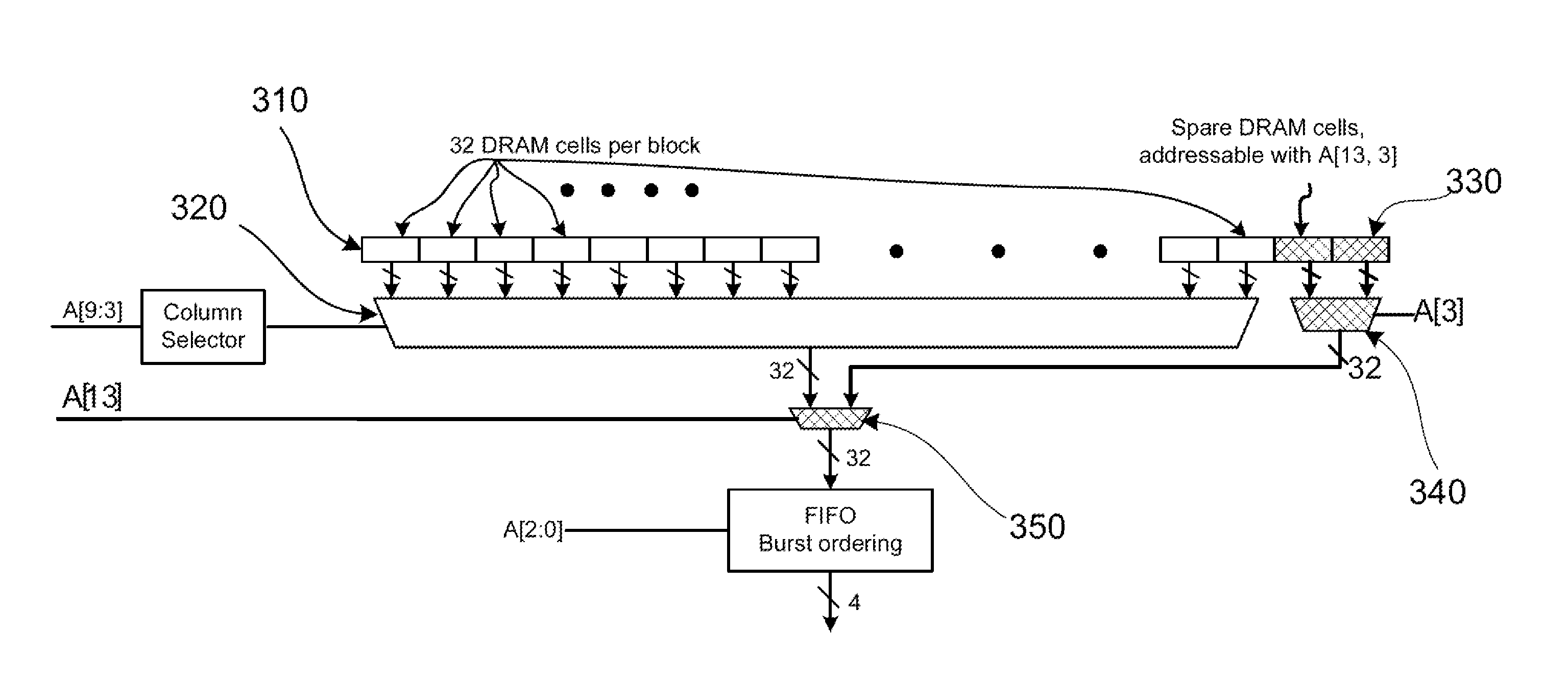
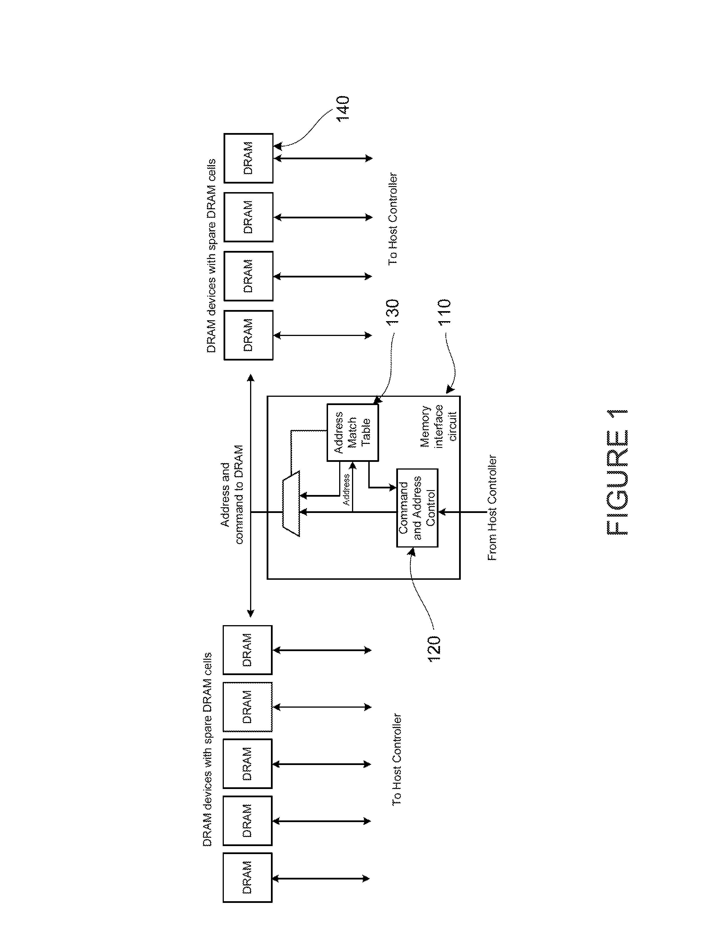
[0034]Utilizing an Address Match Table in Memory Interface Circuit, Controlling Spare Memory Storage Cells to Dynamically Replace Faulty Storage Cells in Memory Devices, as illustrated by FIG. 1.

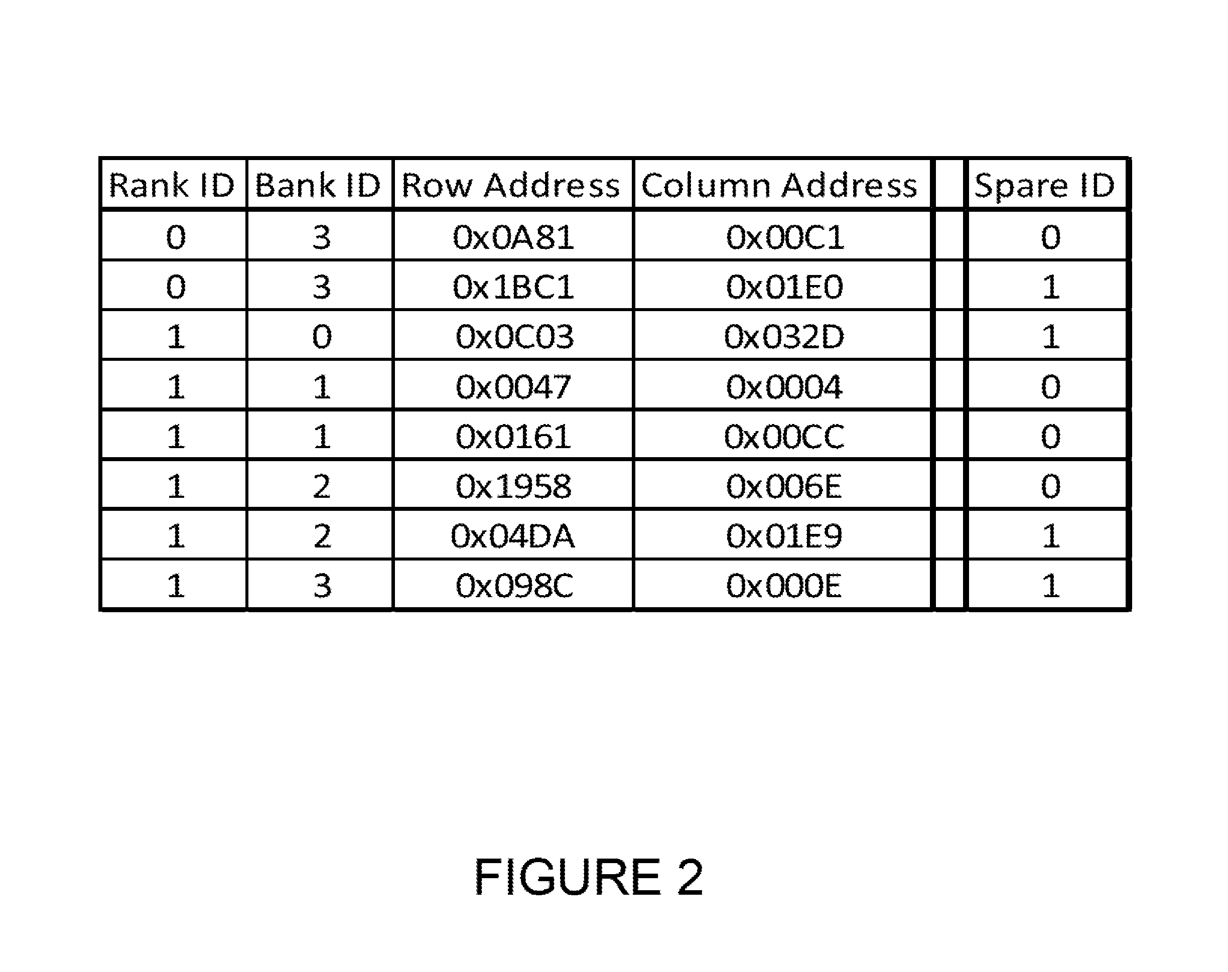
[0035]FIG. 1 shows an example of use of an enhanced interface circuit that, in combination with spare cells in DRAM devices, can function to replace faulty memory locations in the DRAM devices. In FIG. 1, an enhanced memory interface circuit, labeled as 110 is shown to contain a command and address control unit, labeled as 120, and an Address Match Table, labeled as 130. The enhanced memory interface circuit re-drives addresses and commands from the host controller to the DRAM devices, one of which is labeled as 140 in FIG. 1. The DRAM devices contain spare DRAM cells, the addresses of which the enhanced memory interface circuit can select and effect the replacement of faulty or weak storage cell locations, as illustrated by the Table in FIG. 2.

[0036]As an example, the DRAM device may includ...


PUM


Abstract

A memory integrated circuit device is provided. The device includes a plurality of regular address inputs and at least one spare address input configured for a selected mode or an unselected mode. The device includes a plurality of control inputs, a plurality of data inputs, and a plurality of data outputs. The device has a plurality of memory arrays. Each of the memory arrays comprises a plurality of memory cells. Each of the plurality of memory cells is coupled to a data input/output. The device has a spare group of memory cells comprising a plurality of spare memory cells. Each of the plurality of spare memory cells is externally (or internally) addressable using the address match table and configured with the spare address input; whereupon the spare address input is coupled to the address match table to access the spare memory cells.

Description

CROSS-REFERENCES TO RELATED APPLICATIONS[0001]The present application is a continuation-in part application of and incorporates by reference, for all purposes, the following patent application: U.S. Pat. application Ser. No. 13 / 620,288, filed Sep. 14, 2012, which claims priority to U.S. Provisional Application No. 61 / 535,780 filed Sep. 16, 2011.BACKGROUND OF THE DISCLOSURE[0002]The present invention relates generally to solid state memory techniques. More particularly, the present invention provides methods and devices for repairing a “bad memory cell” with a substitute cell for a memory device such as a dynamic random access memory (“DRAM”) device or others.[0003]In memory systems, two general classes of memories exist. Such classes include low latency memories. The low latency memories have effectively infinite endurance or usage-cycles and do not degrade with respect to age or repeated accesses. Additionally, such classes also include relatively longer latency memories that do no...

Claims


Application Information

Patent Timeline
IPC IPC(8): G11C29/04G11C11/24
CPCG11C29/808G11C7/1012G11C11/408G11C11/24G11C29/846G11C29/04G11C11/4093
Inventor WANG, DAVID T.
Owner RAMBUS INC
Why Eureka
Try Eureka