Programmable logic device and method for manufacturing semiconductor device

a logic device and semiconductor technology, applied in the direction of transistors, power consumption reduction, pulse techniques, etc., can solve the problems of inability to accurately estimate the power consumption of a semiconductor device manufactured based on a pld at the stage of testing the pld, and the operation delay and power consumption of parasitic capacitance between various wirings can also not be accurately estimated, so as to reduce the number of elements per bit in a memory array. , the effect of accurately estimated

Active Publication Date: 2013-08-15
SEMICON ENERGY LAB CO LTD
View PDF4 Cites 67 Cited by
  • Summary
  • Abstract
  • Description
  • Claims
  • Application Information

AI Technical Summary

Benefits of technology

[0011]In view of the foregoing technical background, an object of one embodiment of the present invention is to provide a programmable logic device in which the number of elements per bit in a memory array can be reduced. Another object of one embodiment of the present invention is to provide a programmable logic device with which power consumption or operation frequency can be estimated accurately at a testing stage.
[0012]Another object of one embodiment of the present invention is to provide a method for manufacturing a semiconductor device which enables power consumption or operation frequency to be estimated accurately at the stage of testing with a programmable logic device.
[0014]In one embodiment of the present invention, only one transistor, which composes a switch, needs to be provided in each memory element. Therefore, the number of elements per bit can be reduced as compared with the case where an SRAM is used as a memory array.
[0016]In one embodiment of the present invention, a semiconductor device is manufactured by replacement of a memory array provided in the upper layer of a programmable logic device with a plurality of wirings. In one embodiment of the present invention, the memory array of the programmable logic device already includes the plurality of wirings; accordingly, the difference in parasitic capacitance generated between the programmable logic elements in the lower layer and the wirings in the upper layer can be reduced between the programmable logic device and the semiconductor device. Therefore, power consumption or operation frequency of the semiconductor device due to the parasitic capacitance can be estimated accurately by testing of the programmable logic device.
[0017]As another feature of the present invention, a switch provided in a memory element may be composed of a transistor with small off-state current in one embodiment of the present invention. For example, a transistor including, in a channel formation region, a semiconductor which has a wide band gap and is highly purified by reduction of impurities serving as electron donors (donors), such as moisture or hydrogen, and by reduction of oxygen vacancies has extremely small off-state current. In one embodiment of the present invention, the above transistor is used as a switch, whereby leakage of charge held in a node can be prevented. Accordingly, power consumption of the memory array due to the off-state current of a transistor can be reduced as compared with the case where an SRAM composed of polysilicon TFTs is used. Therefore, power consumption of the semiconductor device manufactured based on the programmable logic device can be estimated accurately at the stage of testing the programmable logic device.
[0021]According to one embodiment of the present invention, a programmable logic device in which the number of elements per bit in a memory array can be reduced can be provided. According to one embodiment of the present invention, a programmable logic device with which power consumption or operation frequency can be estimated accurately at a testing stage can be provided. According to one embodiment of the present invention, a method for manufacturing a semiconductor device which enables power consumption or operation frequency to be estimated accurately at the stage of testing with a programmable logic device can be provided.

Problems solved by technology

However, in the configuration of Non-Patent Document 1, the SRAM having a large number of elements per bit is formed over the CMOS logic circuit; thus, defects are likely to be caused, which makes it difficult to manufacture a PLD with high yield.
Moreover, an SRAM composed of polysilicon TFTs not only consumes power in an operating state, but also consumes more than a little power in a non-operating state owing to the off-state current of the polysilicon TFTs, and power consumed by the PLD includes the power consumed by the SRAM.
Therefore, power consumption of a semiconductor device that is manufactured based on the PLD cannot be estimated accurately at the stage of testing the PLD.
Therefore, operation delay and power consumption due to parasitic capacitance between various wirings also cannot be estimated accurately at the stage of testing the PLD.

Method used


Image

  • Programmable logic device and method for manufacturing semiconductor device
  • Programmable logic device and method for manufacturing semiconductor device
  • Programmable logic device and method for manufacturing semiconductor device

Examples


embodiment 1

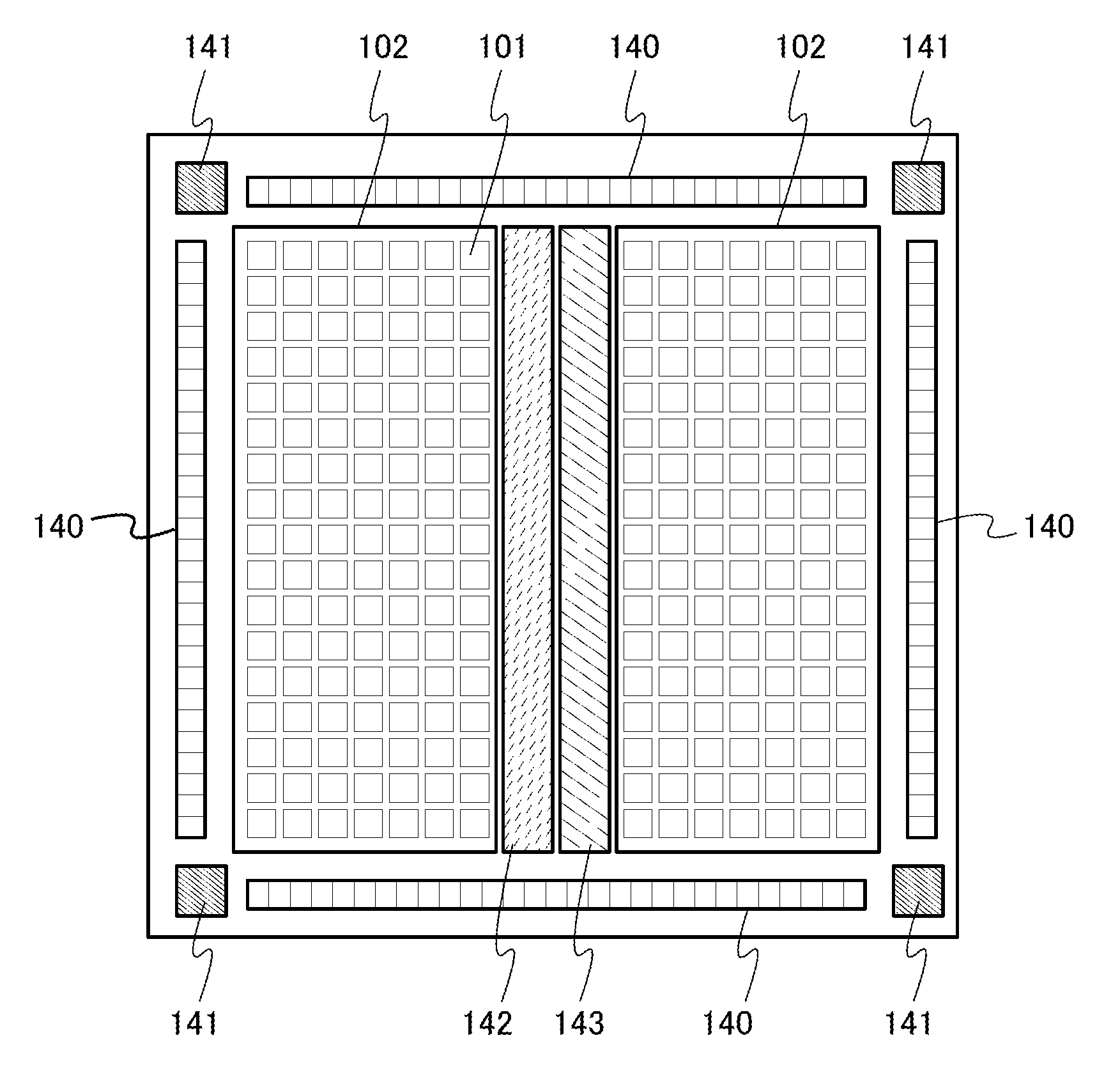
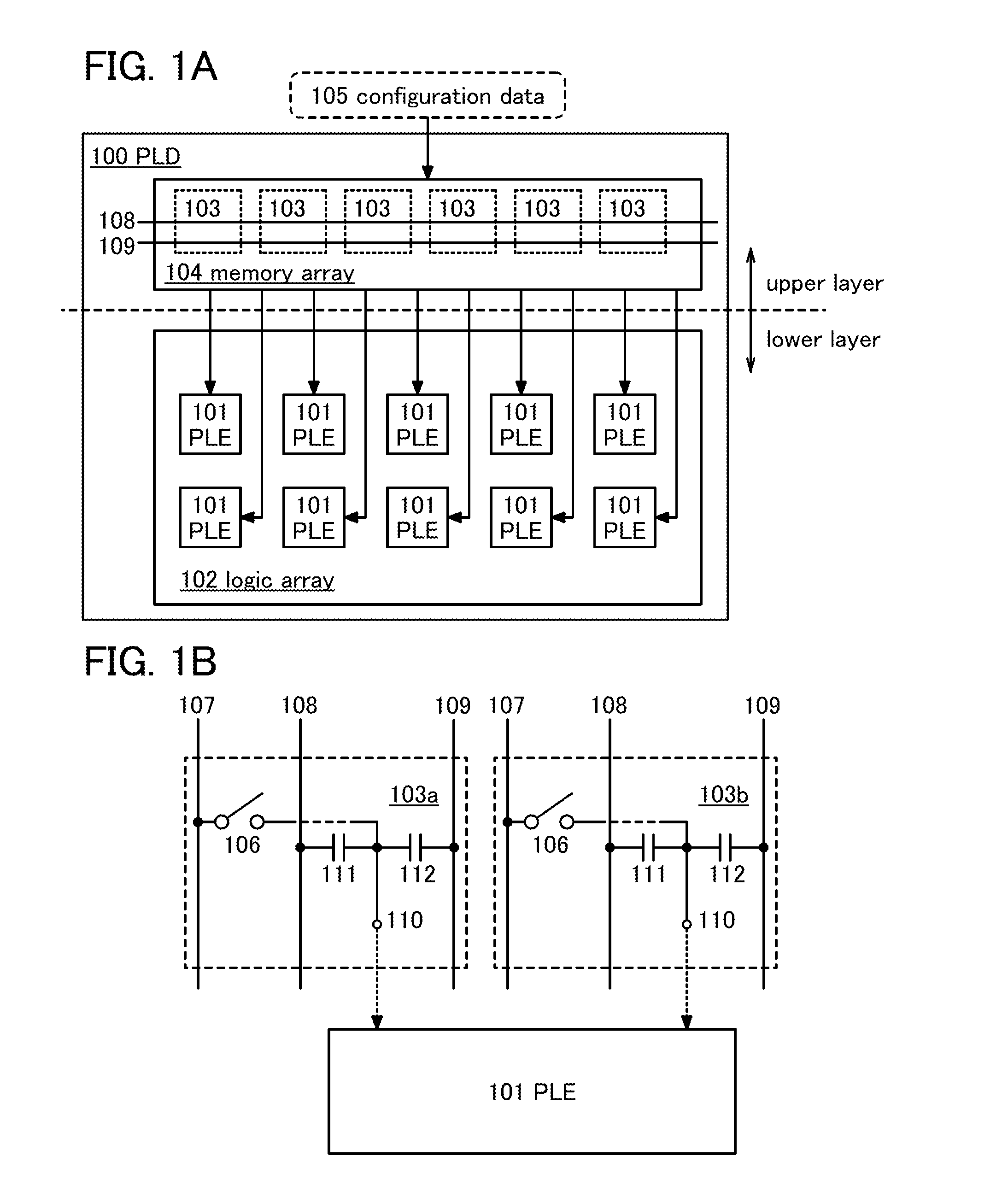
[0044]FIG. 1A schematically illustrates a configuration example of a PLD according to one embodiment of the present invention. A PLD 100 illustrated in FIG. 1A includes a logic array 102 including a plurality of programmable logic elements (PLEs) 101 and a memory array 104 including a plurality of memory elements 103. The memory array 104 is provided over a layer in which the logic array 102 is formed.

[0045]Each PLE 101 is a logic element whose logic operation, i.e., an output value corresponding to an input value, is determined by configuration data 105. Determination of the logic operation executed by each PLE 101 by the configuration data 105 results in determination of the function of a logic circuit that is configured in the logic array 102.

[0046]The memory array 104 has a function of storing the configuration data 105. The memory array 104 is provided with a plurality of wirings for supplying power supply potential to each memory element 103. FIG. 1A illustrates, as an example...

embodiment 2

[0119]In this embodiment, a configuration example of the memory array 104 is described.

[0120]FIG. 8 is a block diagram illustrating a configuration example of the memory array 104. Note that in the block diagram in FIG. 8, circuits in the memory array 104 are classified in accordance with their functions and separated blocks are illustrated. However, it is difficult to classify actual circuits according to their functions completely and it is possible for one circuit to have a plurality of functions.

[0121]The memory array 104 illustrated in FIG. 8 includes a cell array 160 including the plurality of memory elements 103 and a driver circuit 161. The driver circuit 161 includes an input-output buffer 162, a main amplifier 163, a column decoder 164, a row decoder 165, a switch circuit 166, a precharge circuit 167, a sense amplifier 168, and a writing circuit 169.

[0122]The input-output buffer 162 has a function of controlling input of various signals to be used for driving the driver ci...

embodiment 3

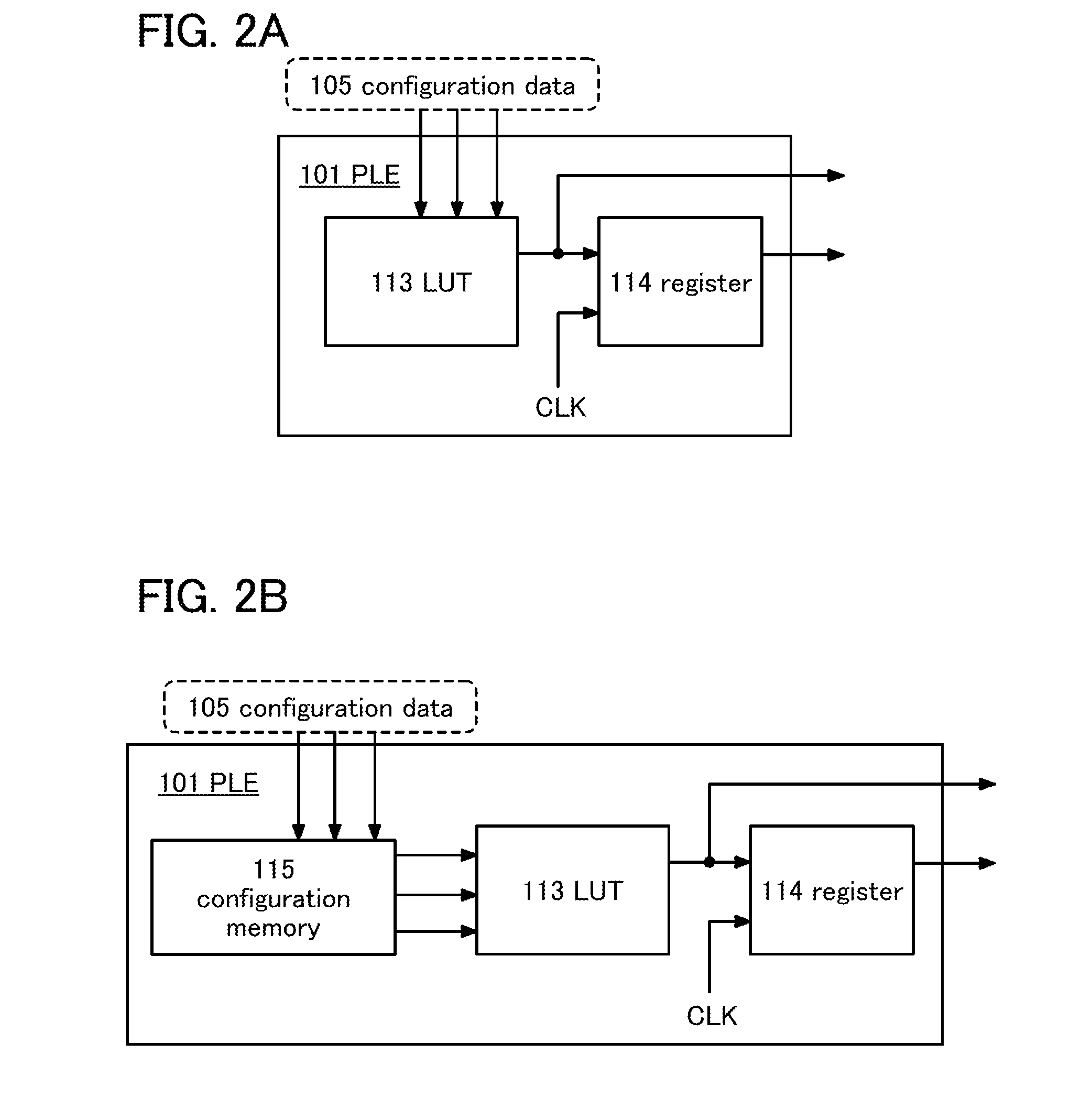
[0154]In this embodiment, a configuration example of the LUT 113 included in the PLE 101 is described. The LUT 113 can be composed of a plurality of multiplexers. Configuration data 105 can be input to any of input terminals and control terminals of the plurality of multiplexers.

[0155]FIG. 11A illustrates one mode of the LUT 113 included in the PLE 101.

[0156]In FIG. 11A, the LUT 113 is composed of seven two-input multiplexers (a multiplexer 31, a multiplexer 32, a multiplexer 33, a multiplexer 34, a multiplexer 35, a multiplexer 36, and a multiplexer 37). Input terminals of the multiplexers 31 to 34 correspond to input terminals M1 to M8 of the LUT 113.

[0157]Control terminals of the multiplexers 31 to 34 are electrically connected to each other and correspond to an input terminal IN3 of the LUT 113. Output terminals of the multiplexers 31 and 32 are electrically connected to two input terminals of the multiplexer 35. Output terminals of the multiplexers 33 and 34 are electrically co...


PUM


Abstract

To provide a programmable logic device in which the number of elements per bit in a memory array can be reduced and with which power consumption or operation frequency can be estimated accurately at a testing stage. Provided is a programmable logic device including a plurality of programmable logic elements and a memory array which stores configuration data that determines logic operation executed in the plurality of programmable logic elements. The memory array includes a plurality of memory elements. The memory element includes a node which establishes electrical connection between the programmable logic element and the memory array, a switch for supplying charge whose amount is determined by the configuration data to the node, holding the charge in the node, or releasing the charge from the node, and a plurality of wirings. Capacitance is formed between the node and the wiring.

Description

BACKGROUND OF THE INVENTION[0001]1. Field of the Invention[0002]The present invention relates to a programmable logic device with which the configuration of hardware can be changed and a method for manufacturing a semiconductor device using the programmable logic device.[0003]2. Description of the Related Art[0004]In a semiconductor device called a programmable logic device (PLD), a logic circuit is composed of an adequate number of programmable logic elements (basic blocks), and the function of each programmable logic element and interconnections between the programmable logic elements can be changed after manufacture. PLDs show flexibility in a reduction in development period and a change in design specification as compared with conventional application specific integrated circuits (ASICs) and gate arrays, which is advantageous, thus being widely used in recent years.[0005]The PLD needs a memory device for storing data (configuration data) on the function of each programmable logi...

Claims


Application Information

Patent Timeline
Patent Type & Authority Applications(United States)
IPC IPC(8): H01L27/105H01L21/82
CPCH03K19/17728H03K19/17748H03K19/1776H01L27/105H01L27/1225H01L27/0207H01L27/11807H01L27/11898H01L21/82H01L28/40H03K19/0008H03K19/1735H03K19/1737H10B10/125H10B10/18
Inventor KUROKAWA, YOSHIYUKI
Owner SEMICON ENERGY LAB CO LTD
Why Eureka
Try Eureka