Semiconductor device having duty-cycle correction circuit

Inactive Publication Date: 2013-08-15
LONGITUDE LICENSING LTD
View PDF7 Cites 9 Cited by
  • Summary
  • Abstract
  • Description
  • Claims
  • Application Information

AI Technical Summary

Benefits of technology

The invention has solved problems with general duty cycle correction circuits, making it possible to control the duty cycle of clock signals with greater accuracy.

Problems solved by technology

However, the general duty-cycle correction circuit mentioned above has some problems explained as follows.
The first problem is that two capacitors with a relatively large capacitance are required.
The second problem is that an analog amplifier circuit is required to detect a potential difference generated between the two capacitors.
While a highly-accurate analog amplifier circuit is required to detect a minute potential difference, it is difficult to obtain the high accuracy due to various factors such as a fluctuation of a threshold value generated between a plurality of transistors.
The third problem is that a discharge operation needs to be performed across a plurality of clock cycles to amplify a potential difference generated between two capacitors, so that it takes time to detect the duty cycle.
The fourth problem is that potentials of capacitors need to be maintained correctly during a discharge operation is performed across clock cycles.
This means that the duty-cycle correction circuit is likely to be affected by noise, which makes it difficult to perform a stable duty-cycle determination operation.
The fifth problem is that, when the duty cycle of the internal clock signal is near 50%, there is little potential difference between two capacitors, which is likely to cause a malfunction of the device.
This problem becomes more conspicuous when the frequency of the internal clock signal is high, because the higher the frequency of the internal clock signal is the shorter a discharge period becomes.
This problem occurs not only in the duty-cycle correction circuit used in a DLL circuit, but also any type of circuit that requires accurate control of the duty cycle of the clock signal.

Method used


Image

  • Semiconductor device having duty-cycle correction circuit
  • Semiconductor device having duty-cycle correction circuit
  • Semiconductor device having duty-cycle correction circuit

Examples


first embodiment

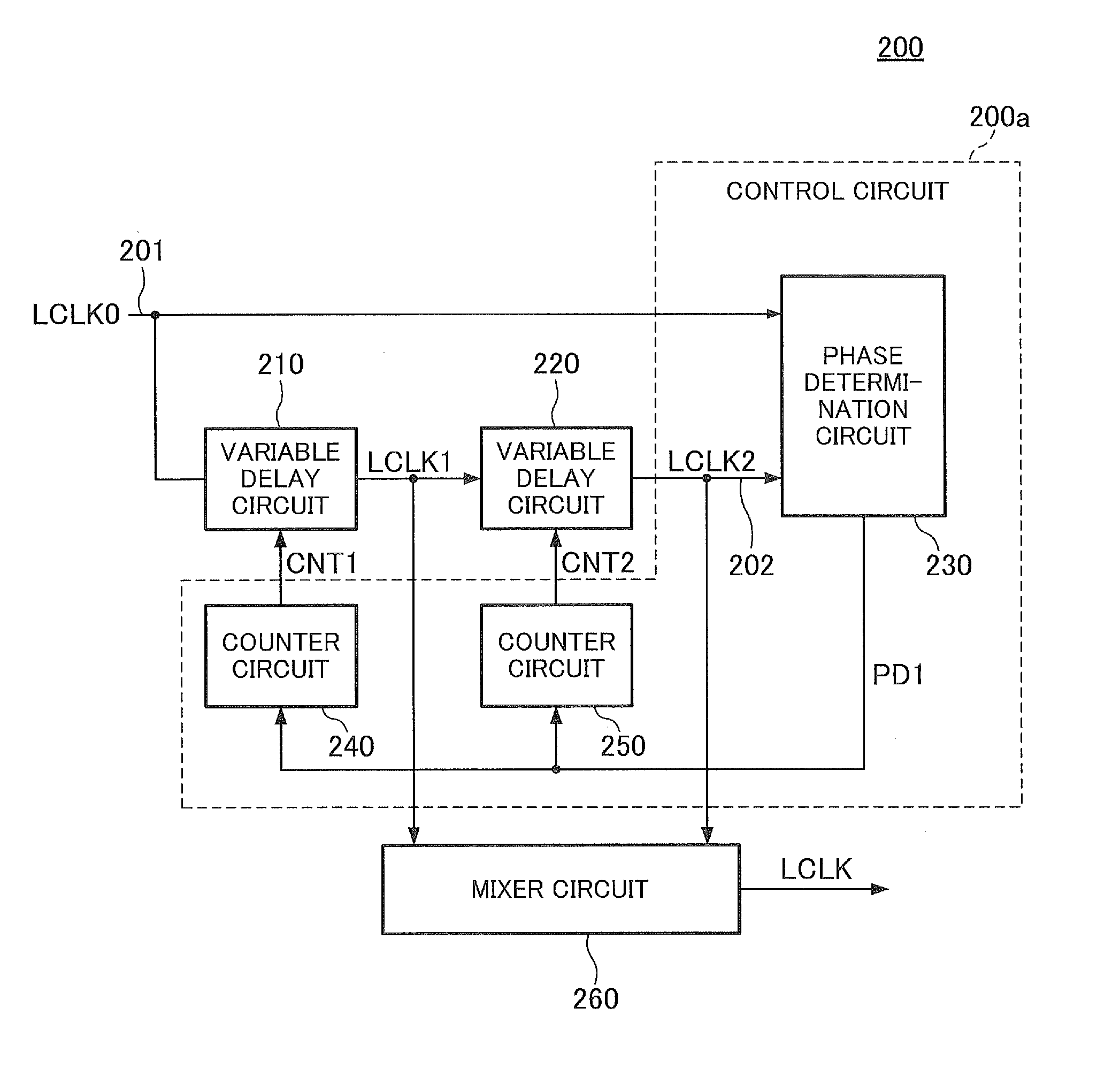
[0039]Referring now to FIG. 1, the semiconductor device 10 according to the present invention is a DRAM and includes the memory cell array 11. In the memory cell array 11, a plurality of word lines WL and a plurality of bit lines BL intersecting with each other are provided and a plurality of memory cells MC are arranged at intersections thereof, respectively. Selection of a word line WL is performed by a row decoder 12 and selection of a bit line BL is performed by a column decoder 13. The bit lines BL are connected to corresponding sense amplifiers SA in a sense circuit 14, respectively, and a bit line BL selected by the column decoder 13 is connected to the amplifier circuit 15 through the corresponding sense amplifier SA.

[0040]Operations of the row decoder 12, the column decoder 13, the sense circuit 14, and the amplifier circuit 15 are controlled by an access control circuit 20. An address signal ADD, a command signal CMD, external clock signals CK and CKB, a clock enable signa...

second embodiment

[0086]If it is assumed that the dead band has a width of 150 ps, the rising edges B to I of the internal clock signal LCLK2 are located in the range of the dead band, where the correct control cannot be performed. That is, even if each of the variable delay circuits 210 and 220 can change the delay amount in the pitch of 10 ps, because the phase determination circuit 230 has the dead band of 150 ps, the accuracy of the variable delay circuits 210 and 220 cannot be utilized effectively. This problem can be solved by performing oversampling by setting the value of m to an integer equal to or larger than 2. the present invention in which the determination accuracy of a phase determination circuit is enhanced by oversampling is explained below.

[0087]Turning to FIG. 18, the duty-cycle correction circuit 400 according to the second embodiment includes 16 variable delay circuits 401 to 416 connected in series. Each of the variable delay circuits 401 to 416 has the same circuit configuratio...


PUM


Abstract

Disclosed herein is a semiconductor device that includes: an input node; an output node; a plurality of variable delay circuits connected in series between the input node and the output node; a control circuit that commonly controls delay amounts of the variable delay circuits based on phases of a first clock signal supplied to the input node and a second clock signal output from the output node; and a mixer circuit that generates a third clock signal based on any one of input clock signals respectively input to the variable delay circuits and any one of output clock signals respectively output from the variable delay circuits.

Description

BACKGROUND OF THE INVENTION[0001]1. Field of the Invention[0002]The present invention relates to a semiconductor device, and more particularly relates to a semiconductor device including a duty-cycle correction circuit.[0003]2. Description of Related Art[0004]In a semiconductor device that performs operations in synchronization with a clock signal, such as a synchronous DRAM (Dynamic Random Access Memory), an internal clock signal that is phase-controlled may be required. The phase-controlled internal clock signal is mainly generated by a DLL (Delay Locked Loop) circuit. In a general DLL circuit, the phase control is performed by adjusting a rising edge timing of the internal clock signal.[0005]Meanwhile, in a DDR (Double Data Rate) DRAM, input and output of data are performed in synchronization with both a rising edge and a falling edge of the internal clock signal, and therefore it is required to accurately control a falling edge timing as well as a rising edge timing. The falling...

Claims


Application Information

Patent Timeline
IPC IPC(8): H03K5/06
CPCH03K5/06H03K5/1506H03K5/1565
InventorKITAGAWA, KATSUHIRO
OwnerLONGITUDE LICENSING LTD