Metal interconnect of semiconductor device and method of manufacturing the same

a technology of metal interconnect and semiconductor device, which is applied in the direction of semiconductor device, semiconductor/solid-state device details, electrical apparatus, etc., can solve the problems of difficult etching of copper, increased unevenness of formed layers, and increased difficulty in achieving etching. , the mechanical strength of the surface of the interlayer insulating film is increased, and the yield of the surface of the metal interconnect is reduced. , the effect of scratches or defects

Inactive Publication Date: 2013-08-22
KOREA INST OF SCI & TECH
View PDF6 Cites 15 Cited by
  • Summary
  • Abstract
  • Description
  • Claims
  • Application Information

AI Technical Summary

Benefits of technology

[0036]According to the metal interconnect of the semiconductor device and the method of manufacturing the same as described above, the mechanical strength of the surface of the interlayer insulating film is increased by performing the nitriding treatment on the surface of the interlayer insulating film, and thus scratches or defects that are generated during the chemical mechanical polishing process involved in the formation of the metal interconnect may be prevented. Therefore, a reduction in yield due to the scratches or defects of the surface of the metal interconnect is improved, and the number of scratches in units of micrometers is reduced, thereby ensuring the reliability of the semiconductor device.
[0037]In addition, the period of use of consumables of a chemical mechanical polishing apparatus is increased, and thus production costs and material costs of the semiconductor device may be reduced. Further, since additional processes and separate facilities for removing scratches or defects that are generated on the surface of the metal interconnect are not required, the manufacturing time and production costs may be reduced.

Problems solved by technology

When such depth of focus is reduced, unevenness of formed layers is increased, and this acts as a fatal factor when lines of succeeding layers are formed.
However, the biggest problem of such techniques is that a degree of planarity corresponding to a required depth of focus may not be ensured as lithography techniques are developed.
However, it is difficult to perform etching on copper.
In the planarization process which is performed using the CMP technique, scratches and various defects are easily generated on the polished surface due to mechanical force generated during the polishing process.
In a case where such scratches and defects are generated during a metal interconnect process which is the final operation of the device manufacturing process, even though all previous device manufacturing processes are perfect, the scratches and defects cause failures due to short circuits of devices and finally have a serious effect on production yields.
However, when consumables of the CMP apparatus are at the last operation, scratches are increased due to the deterioration of the consumables.
However, the scratch spots are vulnerable to reliability evaluation at high temperature and may cause leakage current and short circuits of lines, resulting in malfunction such as an operation stop of semiconductor devices.
However, there is a problem in that additional photolithography / etching processes are needed for removing scratches.

Method used


Image

  • Metal interconnect of semiconductor device and method of manufacturing the same
  • Metal interconnect of semiconductor device and method of manufacturing the same
  • Metal interconnect of semiconductor device and method of manufacturing the same

Examples


Embodiment Construction

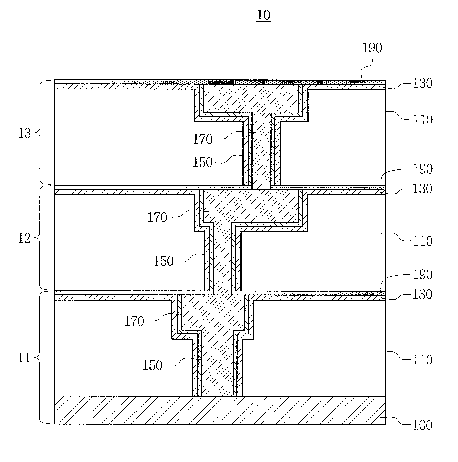
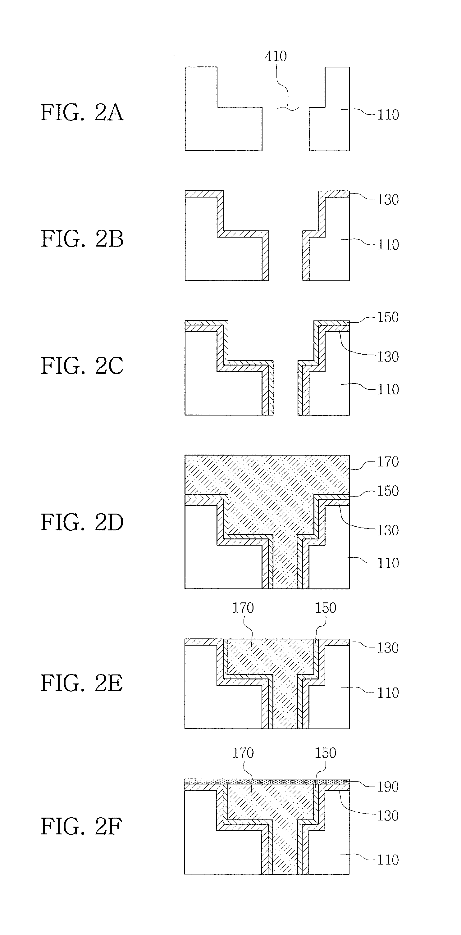
of Main Elements] 10: metal interconnect100: substrate110: interlayer insulating film130: hardness controlled unit150: diffusion preventing film170: metal190: protective film410: interconnect hole 20: deposition apparatus

DETAILED DESCRIPTION

[0044]Hereinafter, exemplary embodiments of a metal interconnect of a semiconductor device and a method of manufacturing the same according to the disclosure will be described in detail with reference to the drawings.

[0045]FIG. 1 is a cross-sectional view of a metal interconnect of a semiconductor device according to an exemplary embodiment of the disclosure.

[0046]Referring to FIG. 1, the metal interconnect 10 of the semiconductor device according to the exemplary embodiment of the disclosure includes: an interlayer insulating film 110 in which a interconnect hole is formed; a hardness controlled unit 130 which is formed on the upper portion of the interlayer insulating film 110 and in the vicinity of the interconnect hole; a diffusion preventing...


PUM

PropertyMeasurementUnit
peak voltageaaaaaaaaaa
temperatureaaaaaaaaaa
peak voltageaaaaaaaaaa

Abstract

Provided is a method of manufacturing a metal interconnect of a semiconductor device including: forming a interconnect hole by patterning an interlayer insulating film formed on a substrate; performing a nitriding treatment on a surface of the interlayer insulating film by injecting a gas including nitrogen into a deposition apparatus in which the substrate is disposed; forming a diffusion preventing film by injecting the gas including nitrogen and a metal source gas into the deposition apparatus together; filling the interconnect hole with a metal; and removing the metal formed on a part other than the interconnect hole by a chemical mechanical polishing (CMP) process. Accordingly, the mechanical strength of the interlayer insulating film is increased, thereby preventing scratches or defects that are generated during the chemical mechanical polishing process.

Description

CROSS-REFERENCE TO RELATED APPLICATION[0001]This application claims priority to Korean Patent Application No. 10-2012-0015689, filed on Feb. 16, 2012, and all the benefits accruing therefrom under 35 U.S.C. §119, the contents of which in its entirety are herein incorporated by reference.BACKGROUND[0002]1. Field[0003]The following disclosure relates to a metal interconnect of a semiconductor device and a method of manufacturing the same, and in particular, to a metal interconnect of a semiconductor device having improved reliability and a method of manufacturing the same.[0004]2. Description of the Related Art[0005]For an increase in the degree of integration and performance improvement of a semiconductor integrated circuit, minute line widths have been demanded when devices are manufactured. In addition, metal interconnects in circuits need 6 to 7 or more layers in the case of logic circuits, and such a multi-layer line structure has been popularized.[0006]In order to form minute li...

Claims


Application Information

Patent Timeline
Patent Type & Authority Applications(United States)
IPC IPC(8): H01L23/48H01L21/768
CPCH01L23/53238H01L23/5329H01L23/53295H01L21/76843H01L21/76826H01L21/76831H01L21/7684H01L21/76814H01L2924/0002H01L2924/00H01L21/28
Inventor KIM, YOUNG HWANKIM, YONG TAEKIM, SEONG ILKIM, CHUN KEUN
Owner KOREA INST OF SCI & TECH
Why Eureka
Try Eureka