Semiconductor device
a technology of semiconductors and capacitors, applied in the direction of solid-state devices, transistors, instruments, etc., can solve the problems of insufficient power consumption reduction, frequent refresh operation, and extremely short retention period, and achieve the effect of reducing area and low power
- Summary
- Abstract
- Description
- Claims
- Application Information
AI Technical Summary
Benefits of technology
Problems solved by technology
Method used
Image

Examples
embodiment 1
[0071]In this embodiment, as an example of a semiconductor device of an embodiment of the present invention, an example of a structure of a memory device will be described with reference to drawings.
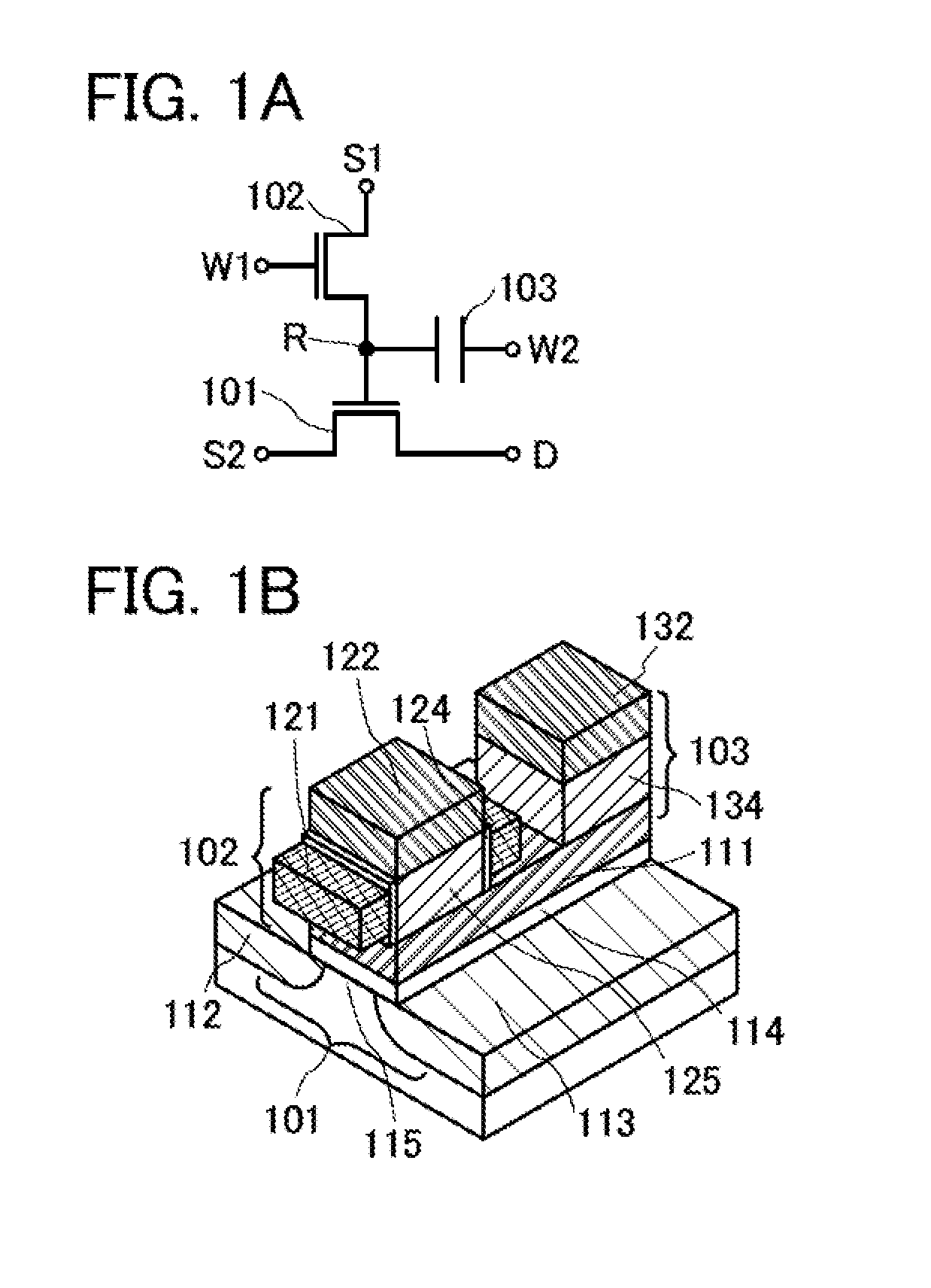
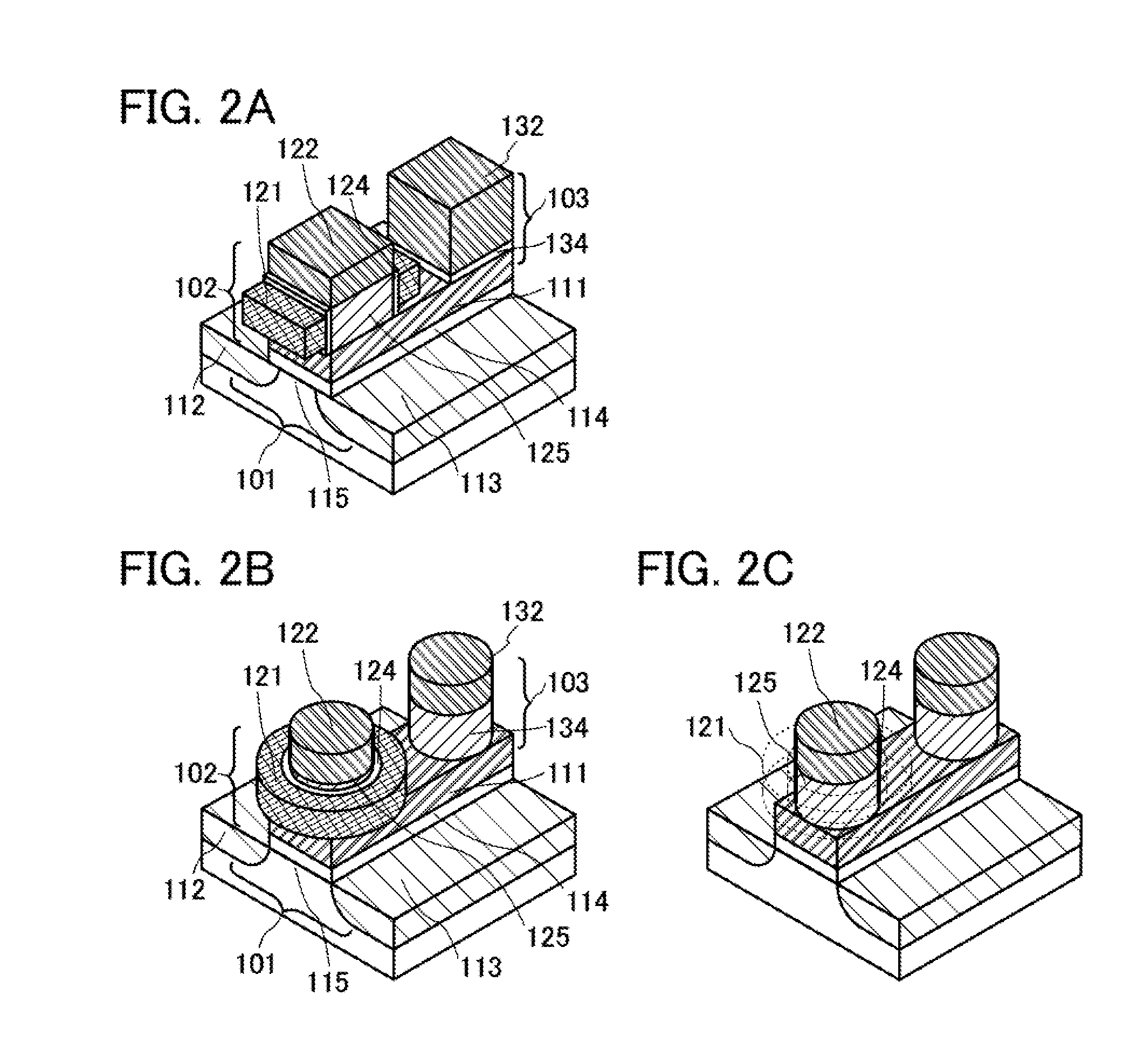
[0072]FIG. 1A is a circuit diagram of a main portion of the memory device of an embodiment of the present invention. The memory device includes a transistor 101, a transistor 102, and a capacitor 103.
[0073]The memory device includes a node (holding node R) to which a gate electrode of the transistor 101, a first electrode of the transistor 102, and one electrode of the capacitor 103 are electrically connected.
[0074]A wiring S2 is electrically connected to a first electrode of the transistor 101 and a wiring D is electrically connected to a second electrode of the transistor 101. A wiring W1 is electrically connected to a gate electrode of the transistor 102 and a wiring S1 is electrically connected to a second electrode of the transistor 102. A wiring W2 is electrically connected to the ...
embodiment 2
[0100]In this embodiment, as an example of a semiconductor device of an embodiment of the present invention, another example of a structure of a memory device will be described with reference to drawings. Note that description of the same portions as those in the above embodiment is omitted or simplified.
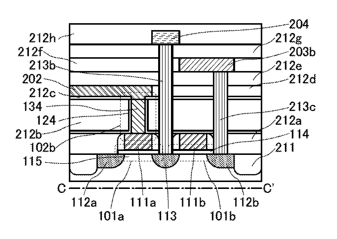
[0101]FIG. 3A is a circuit diagram of a main portion of the memory device which is described as an example in this embodiment.
[0102]Here, one memory element includes two transistors and one capacitor.
[0103]The memory device illustrated in FIG. 3A includes a memory element 110a including a transistor 101a, a transistor 102a, and a capacitor 103a and a memory element 110b including a transistor 101b, a transistor 102b, and a capacitor 103b. The structures of the memory elements 110a and 110b can be similar to that of the memory device described in Embodiment 1.
[0104]In the memory device, the wiring W1 is electrically connected to gates of the transistor 102a and the transistor 102b, t...
embodiment 3
[0238]In this embodiment, as an example of a semiconductor device of an embodiment of the present invention, an example of a structure of a memory device which is different from the memory devices of the above embodiments will be described with reference to drawings. Note that description of the same portions as those in the above embodiments is omitted or simplified.
[0239]FIG. 12A is a circuit diagram of a main portion of the memory device described in this embodiment.
[0240]The memory device includes the transistor 101, the transistor 102, and the capacitor 103.
[0241]In the memory device, the wiring S1 is electrically connected to the first electrodes of the transistor 101 and the transistor 102, the wiring S2 is electrically connected to the second electrode of the transistor 101, the wiring W1 is connected to the gate of the transistor 102, and the wiring W2 is electrically connected to one electrode of the capacitor 103.
[0242]FIG. 12B is a schematic top view of the memory device...
PUM
 Abstract
Description
Claims
Application Information
 - R&D
- Intellectual Property
- Life Sciences
- Materials
- Tech Scout
- Unparalleled Data Quality
- Higher Quality Content
- 60% Fewer Hallucinations
Browse by: Latest US Patents, China's latest patents, Technical Efficacy Thesaurus, Application Domain, Technology Topic, Popular Technical Reports.
© 2025 PatSnap. All rights reserved.Legal|Privacy policy|Modern Slavery Act Transparency Statement|Sitemap|About US| Contact US: help@patsnap.com